Publication
- Physical Insights into Vacancy-Based Memtransistors: Toward Power Efficiency, Reliable Operation, and Scalability

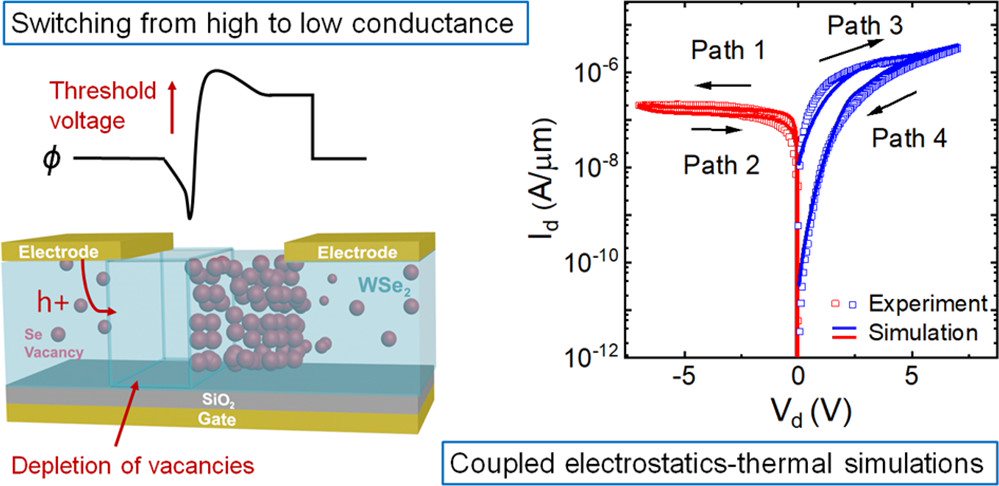
Memtransistors that combine the properties of transistor and memristor hold significant promise for in-memory computing. While superior data storage capability is achieved in memtransistors through gate voltage-induced conductance modulation, the lateral device configuration would not only result in high write bias, which compromises the power efficiency, but also suffers from unsuccessful memory reset that leads to reliability concerns. To circumvent such performance limitations, an advanced physics-based model is required to uncover the dynamic resistive switching behavior and deduce the key driving parameters for the switching process. This work demonstrates a self-consistent physics-based model which incorporates the often-overlooked effects of lattice temperature, vacancy dynamics, and channel electrostatics to accurately solve the interaction between gate potential, ions, and carriers on the memristive switching mechanism. The completed model is carefully calibrated with an ambipolar WSe2 emtransistor and hence enables the investigation of the carrier polarity effect (electrons vs holes) on vacancy transport. Nevertheless, the validity of the model can be extended to different materials by a simple material-dependent parameter modification. Building upon the existing understanding of Schottky barrier height modulation, our study reveals three key insights─leveraging threshold voltage shifts to lower write bias; optimizing lattice temperature distribution and read bias polarity to achieve successful memory state recovery; engineering contact work function to overcome the detrimental parasitic current flow in short channel ambipolar memtransistors. Therefore, understanding the significant correlation between the switching mechanisms, different material systems, and device structures allows performance optimization of operating modes and device designs for future memtransistors-based computing systems.
Researcher/Author: Maheswari Sivan, Jin Feng Leong, Joydeep Ghosh, Baoshan Tang, Evgeny Zamburg, Aaron Voon-Yew Thean
- Home
- Physical Insights into Vacancy-Based Memtransistors: Toward Power Efficiency, Reliable Operation, and Scalability
Singapore Hybrid-Integrated Next-Generation μ-Electronics (SHINE) Centre
- Block E6, #E6-5-3, 5 Engineering Drive 1, Singapore 117608
- +65 6601 8522
- shine@nus.edu.sg

