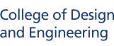
The SHINE management was delighted to welcome Dr. Gaurav Thareja, Director & Head of Logic & Memory Process Integration in the Metals Deposition Products Division of the Semiconductor Products Group (SPG) at Applied Materials, to the NUS campus on 28 June 2024. Dr. Thareja delivered an insightful talk titled “The Logic Technology Roadmap for the Trillion Transistor Era”.
Some of the key advancements he shared included:
Scaled GAA (Gate-all-around) NS CMOS: Expected for upcoming nodes, this technology enables further miniaturization and performance enhancements.
CFET (Complementary FET): Offers significant advantages for continued scaling, pushing the boundaries of semiconductor technology.
AI-Enabled Semiconductor Manufacturing: Accelerates AI chip production through AI/ML techniques, facilitating materials discovery, equipment design, process recipe optimization, and digital twin technology.
Dr. Thareja ended the talk on a positive note, highlighting the bright future of Logic CMOS driven by the AI revolution, which is fostering new catalysts and opportunities for innovations in next-generation computing.
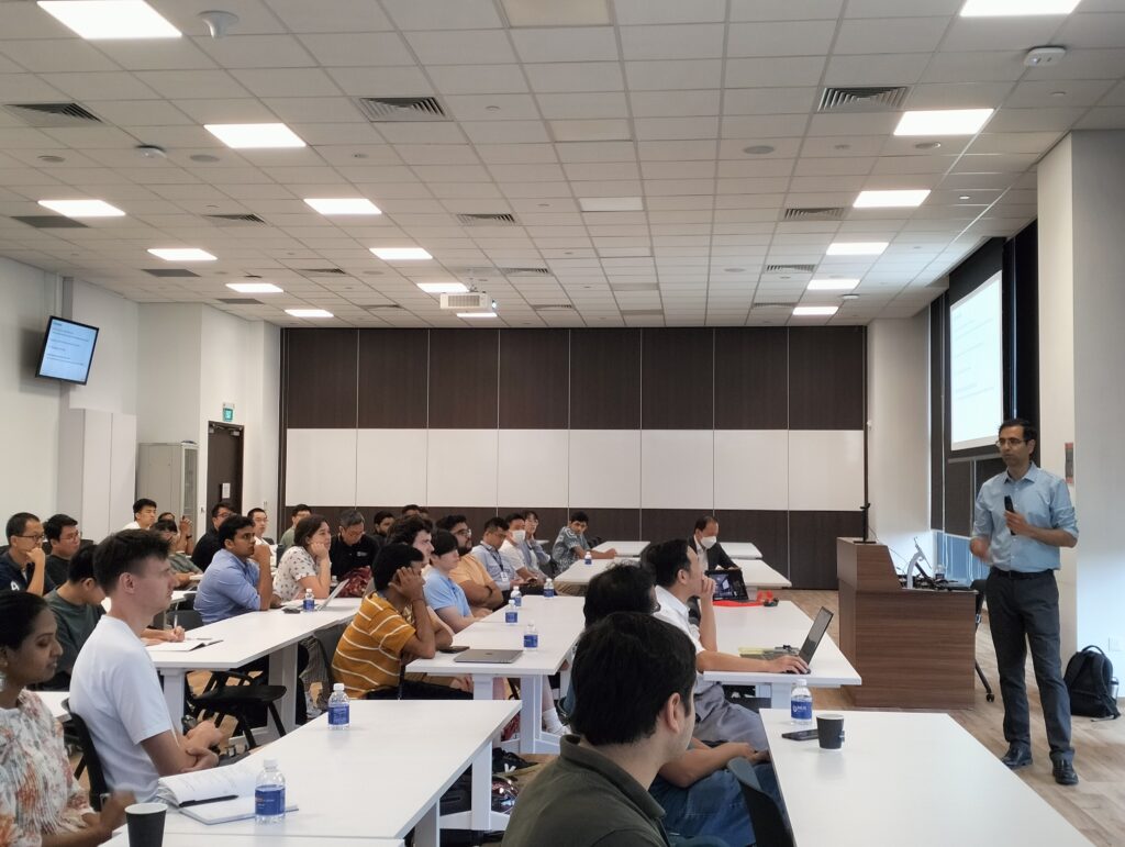
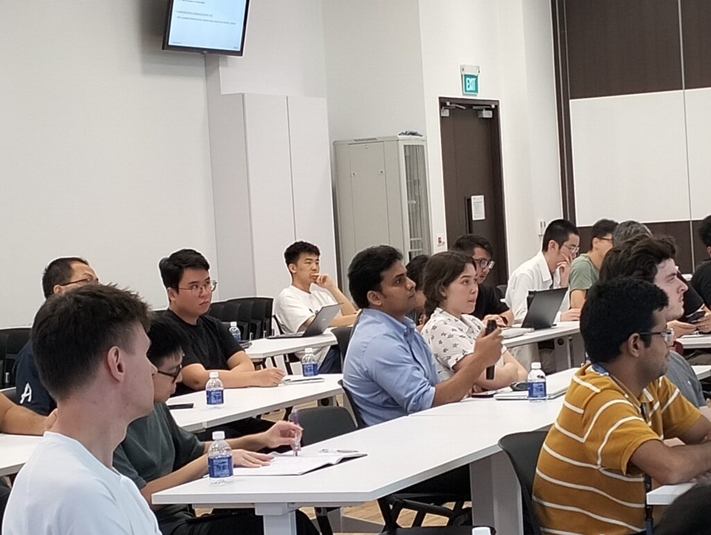
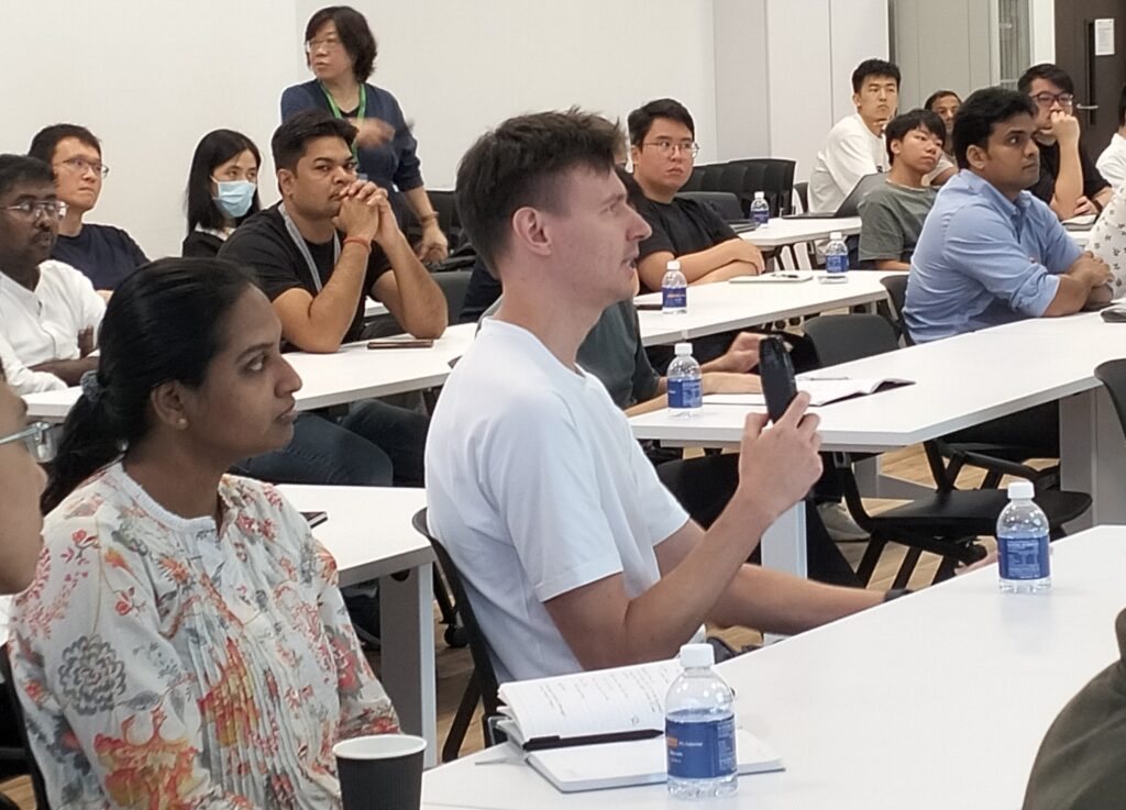
Numerous questions from the audience reflected their keen interest and enthusiasm. We are grateful to Dr. Thareja for sharing his expertise and insights. The talk undoubtedly enriched our understanding of the future trajectory of semiconductor technology and its exciting possibilities.