SHINE ZEISS Joint Seminar | 13 March 2025
Exploring Defects and Structures. Microscopy Solutions for Advanced Semiconductor Packaging
On 13th March, the NUS SHINE & ZEISS Joint Seminar on Non-Destructive 3D Imaging and AI-Driven Deep Learning for Semiconductor Materials drew close to 55 attendees, providing a deep dive into the latest advancements in semiconductor failure analysis.
The event commenced with an opening address by Prof. Lim Yeow Kheng, Programme Director of SHINE who emphasized that failure analysis is a crucial aspect of the semiconductor industry and that researchers must think ahead of their time. He highlighted the growing importance of AI-enhanced imaging in semiconductor research, which accelerates failure analysis. He encouraged attendees to make the most of the sharing session by learning and exchanging information.
The seminar featured expert speakers from academia and industry, offering insights into how X-ray Computed Tomography (CT), machine learning (ML), and correlative microscopy are transforming defect detection, predictive diagnostics, and material characterization.
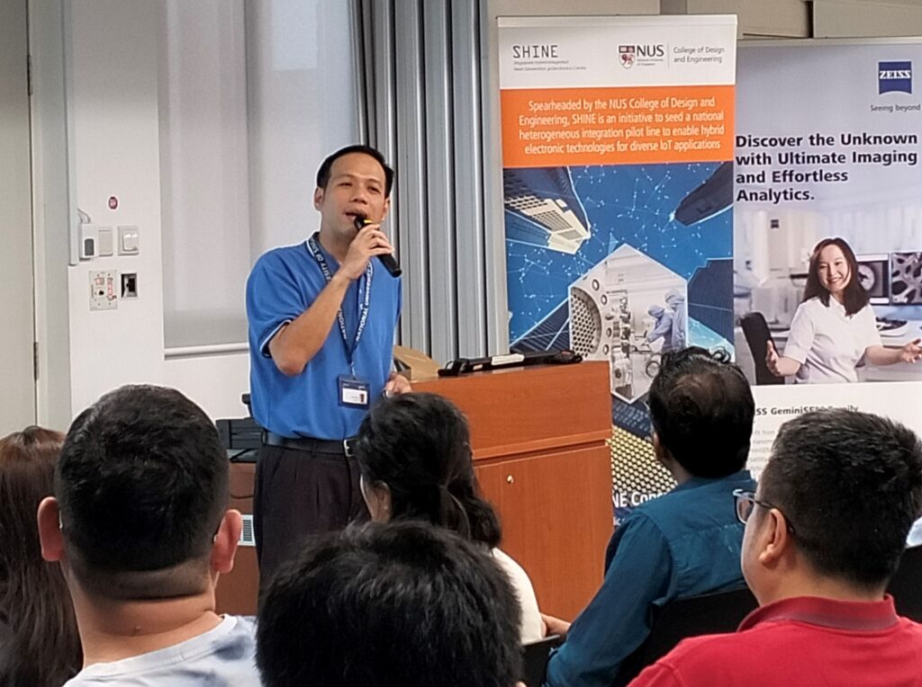
The seminar’s technical discussions covered a range of innovative methodologies:
- Dr. Sky Xie, ZEISS Research Microscopy Solutions Sales Specialist, introduced deep-learning-enhanced X-ray CT, showcasing its ability to improve imaging efficiency while preserving defect details.
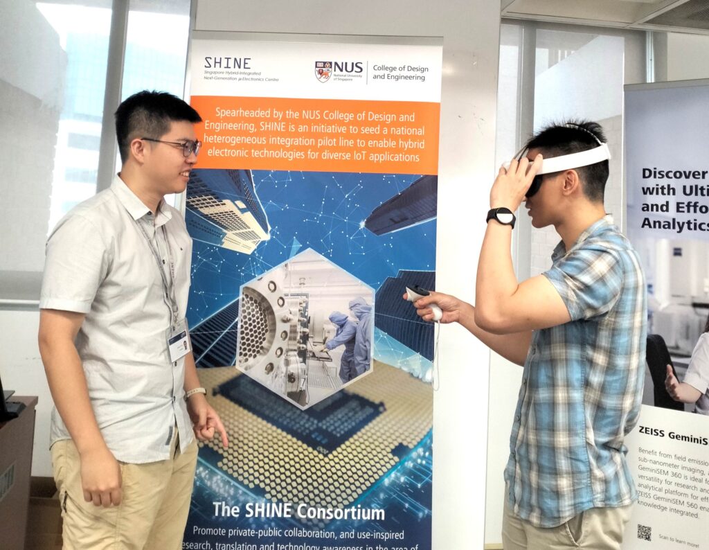
- Mr. Shi Zhansen, Research Engineer at NUS SHINE Centre, explored the integration of X-ray imaging with machine learning to advance electronic digital twins, enabling precise defect localization and circuit reconstruction. His talk also featured a VR demonstration, offering an immersive perspective on circuit analysis and reconstruction.
- Dr. Riko I Made, Scientist at A*STAR, discussed the role of ML in X-ray CT for automated defect detection and predictive failure modeling.
- Dr. Feng Lin Ng, APAC Materials Research and Research Microscopy Solutions Business Development Specialist at ZEISS, demonstrated a correlative microscopy workflow that bridges multi-scale imaging techniques for targeted semiconductor research.
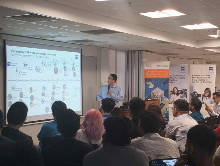
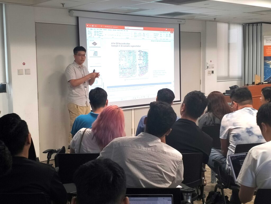
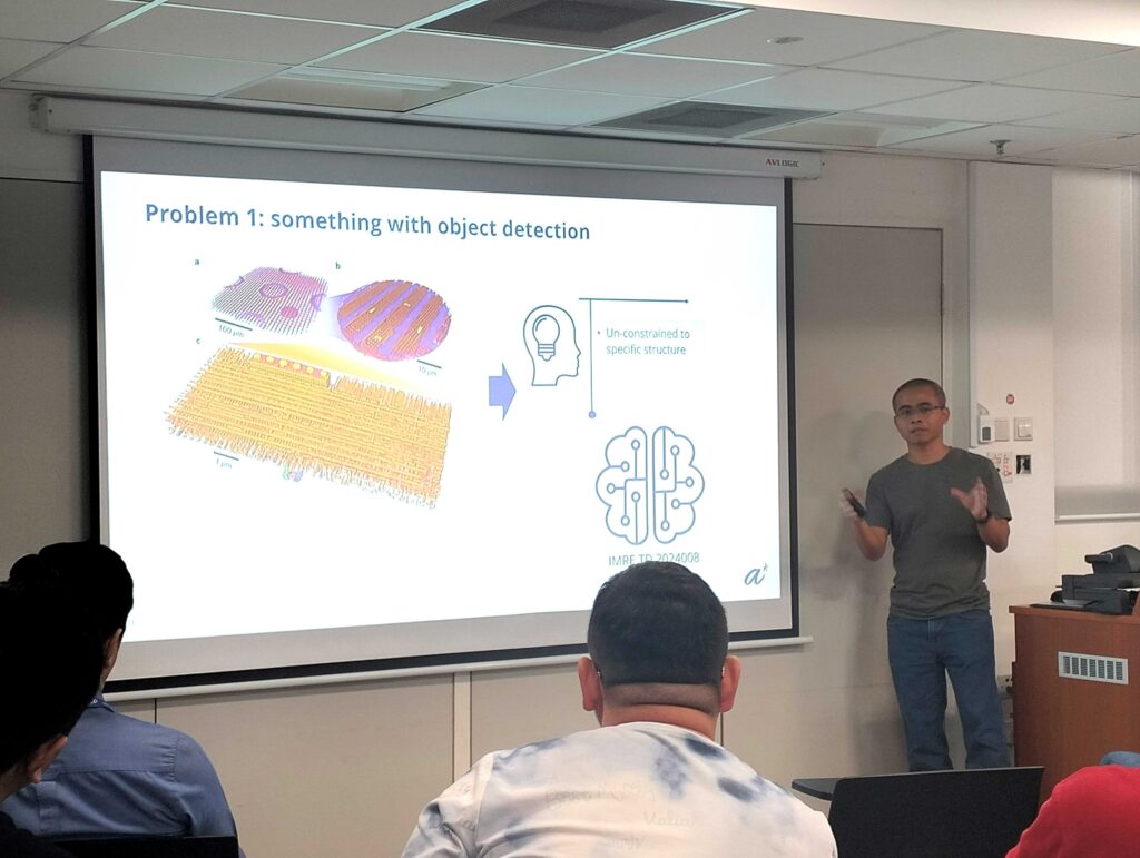
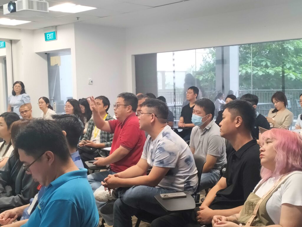
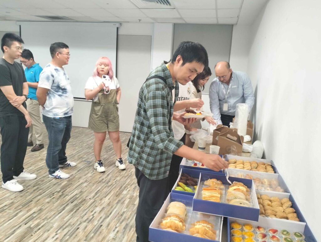
The seminar provided a platform for meaningful discussions and cross-disciplinary collaborations, with participants engaging in thought-provoking exchanges on the future of AI-driven imaging in semiconductor diagnostics. The event concluded with an interactive quiz, reinforcing key takeaways from the presentations.
- Home
- SHINE ZEISS Joint Seminar: Exploring Defects & Structures. Microscopy Solutions for Advanced Semiconductor Packaging
Singapore Hybrid-Integrated Next-Generation μ-Electronics (SHINE) Centre
- Block E6, #E6-5-3, 5 Engineering Drive 1, Singapore 117608
- +65 6601 8522
- shine@nus.edu.sg
