On-Chip Circuit Harness Enabling Probe-Less, Position-Invariant and Massive Testing of Chiplets via Die Front/Back-Side Capacitive Coupling
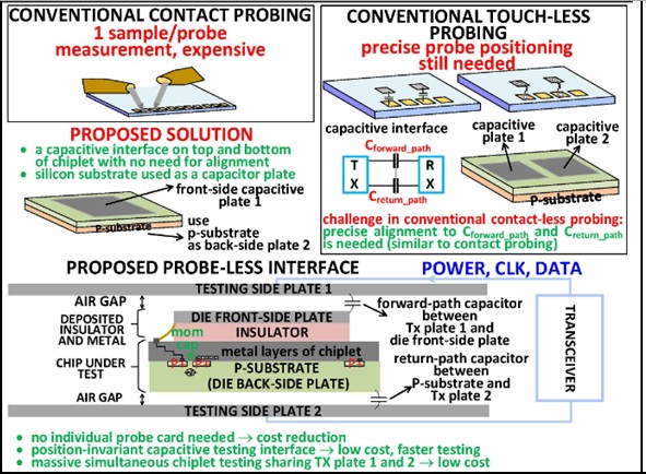
Modern integrated circuit design often involves integrating multiple smaller, specialized dies (often called chiplets or tiles) into a single package. This approach, known as chiplet-based integration or 3D integration [1], enables the creation of complex, high-performance, and cost-effective systems. Heterogeneously integrated systems based on chiplets invariably require an extra testing/screening step for individual chiplets before integration and full-system testing. This creates a fundamental challenge in ultra-low power (∼μW) and low cost systems (few tens of cents) for the loT, whose total testing budget is generally limited to a few cents. Hence, innovation at the boundary of testing equipment and chiplets is needed to significantly reduce chiplet testing cost over traditional testing approaches.