News Highlights
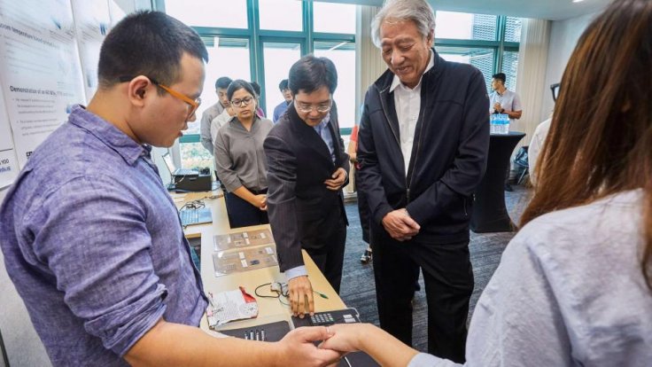
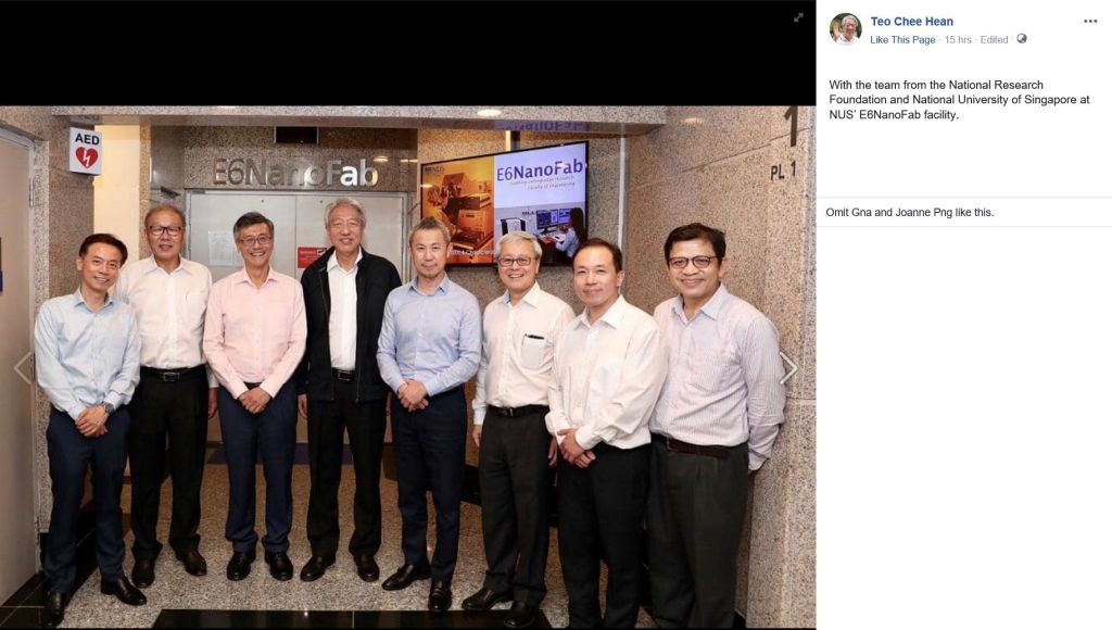
Deputy Prime Minister Teo Chee Hean visited E6NanoFab, which is an integrated research and development facility at NUS Engineering March 20. NUS President Professor Tan Eng Chye and NUS Deputy President (Research and Technology) Professor Chen Tsuhan, as well as representatives from the National Research Foundation and NUS Engineering also joined him.
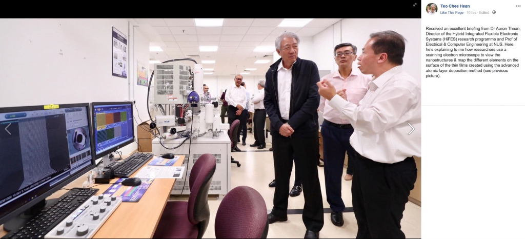
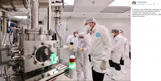
E6NanoFab includes class 10, class 100, class 1000 and class 10,000 cleanrooms. During the visit of DPM Teo, Professor Aaron Thean, Director of E6NanoFab gave him an overview of the state-of-the-art cleanroom facilities and advanced process and material characterisation capabilities offered by the nanofabrication facility.
Prof Thean is also the Director of the Hybrid Integrated Flexible Electronic Systems (HiFES) programme, which is an initiative, taken by NUS and Faculty of Engineering to spearhead innovations in hybrid flexible electronics.
He is also Co-director of the Applied Materials-NUS Advanced Materials Corporate Lab (AMAT-NUS Advanced Materials Corporate Lab) that combines Applied Materials’ leading expertise in materials engineering and semiconductor technologies with NUS’ world-class and multi-disciplinary R&D capabilities that span applied chemistry, materials science and microelectronics process engineering.
Prof Thean shared with DPM Teo the current projects and research progress under the programme and at the laboratory.
“Hosted in E6NanoFab, the HiFES programme seeks to spearhead innovations in hybrid flexible electronics while the AMAT-NUS Advanced Materials Corporate Lab aims to accelerate the discovery and commercialisation of new materials for manufacturing next-generation semiconductors,” the statement added.
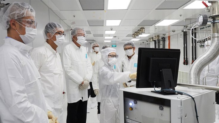
DPM Teo, the member of the governing People’s Action Party, visited a cleanroom that houses advanced atomic layer processing equipment essential for the production of next-generation semiconductor electronics. He was given a demonstration of how the image of a nanoscale structure can be “characterised” or viewed with scanning electron microscopes (SEM) in the SEM Characterisation Laboratory.
The Researchers and staff from the HiFES programme also communicated with DPM Teo and shared their projects and work experience with him.
This article is published by International Business Times on 27 March 2019.
https://www.ibtimes.sg/education-deputy-pm-teo-chee-hean-visits-e6nanofab-nus-engineering-30059