Asian Deans’ Forum Visit to SHINE Centre November 18, 2024
Asian Deans’ Forum Visit to SHINE Centre
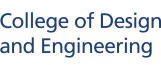
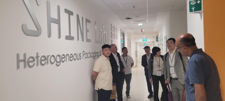
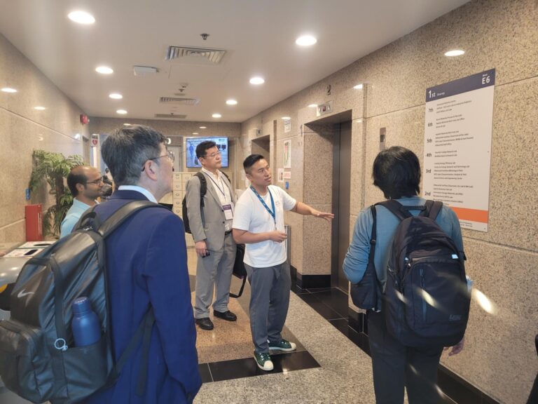
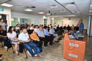
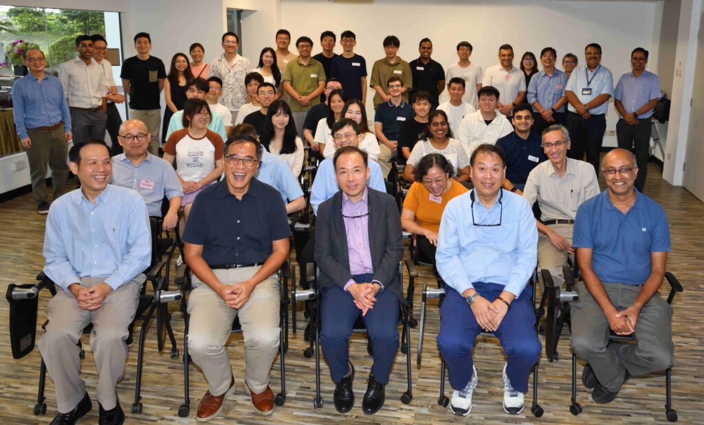
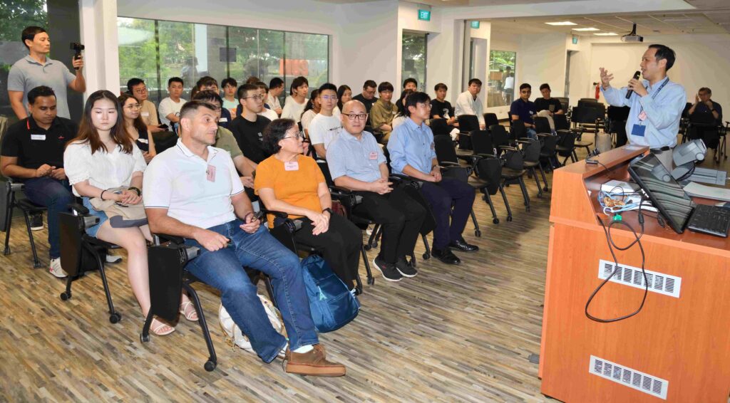
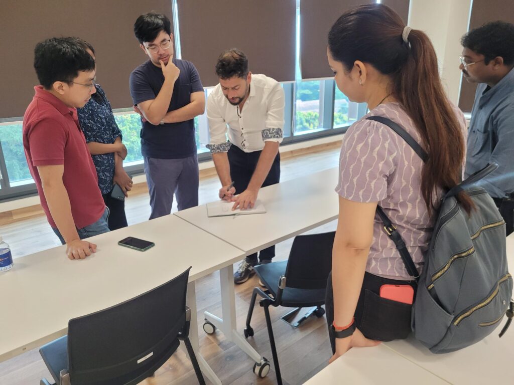
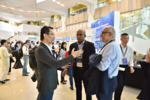
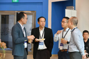
SHINE proudly hosted participants from the Asian Deans’ Forum 2024 on 18 November, offering them an exclusive look into our advanced nanofabrication and microelectronics facilities.
The Asian Deans’ Forum 2024 – The Rising Stars Women in Engineering Workshop, organized by Asia’s top engineering institutions and hosted by the National University of Singapore, aims to unite young women professionals in engineering from around the globe. This workshop fosters collaboration among scholars, researchers, and engineers pursuing academic careers, while serving as a platform for scientific and career-focused discussions that empower women academic leaders in Asia.
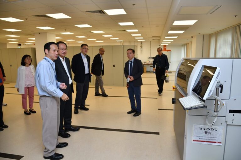
Dr. David Xu, Process Engineering Research Lead, kicked off the visit with an engaging overview of SHINE and E6NanoFab’s capabilities. Participants explored our cleanrooms of varying classifications and dry labs, gaining insights into cutting-edge technologies in deposition, lithography, metrology, characterization, and packaging.
We extend our deepest gratitude to the dedicated team of researchers, engineers, and laboratory officers at the Packaging Facilities @ SHINE Centre and E6NanoFab for their exceptional efforts in making the tour a resounding success.
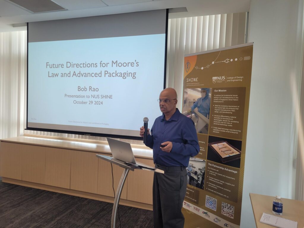
SHINE Overseas Speaker Series Workshop on “Future Directions for Moore’s Law and Advanced Packaging October 29, 2024
SHINE Overseas Speaker Series Workshop: Future Directions for Moore’s Law and Advanced Packaging | 29 Oct 2024
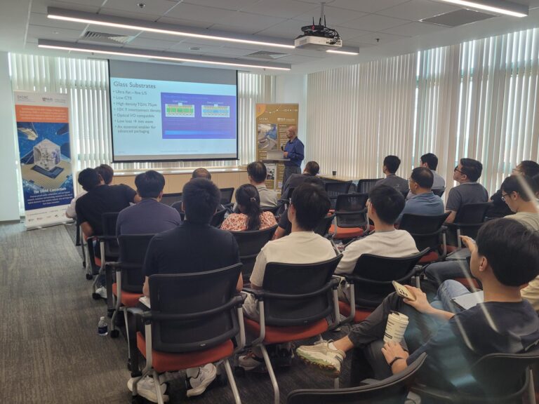
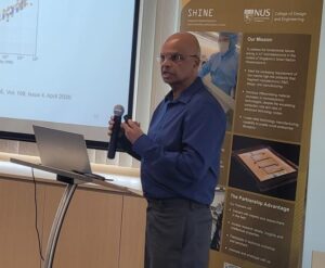
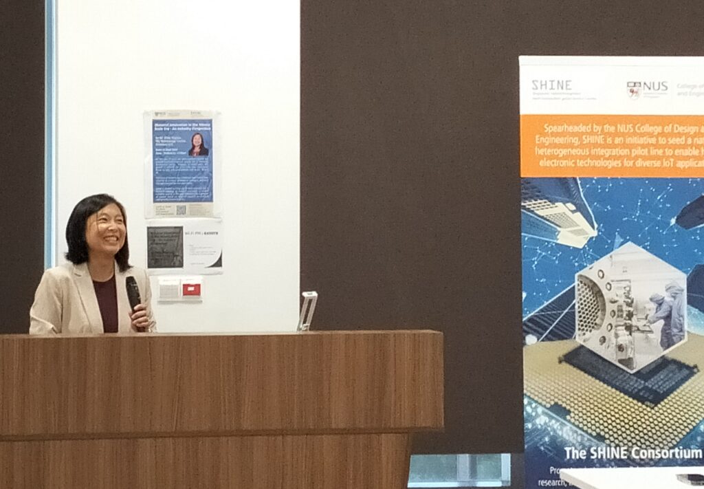
On 29 October 2024, SHINE held an insightful Overseas Speaker Series Workshop featuring Dr. Valluri (Bob) Rao, a renowned independent consultant, former Intel Fellow and IEEE Fellow. Dr. Rao’s presentation, “Future Directions for Moore’s Law and Advanced Packaging,” explored the urgent challenges and technological innovations needed to support the future demands of semiconductor scaling, particularly in the era of Artificial Intelligence (AI) and Large Language Models (LLMs).
Key Takeaways
The presentation highlighted the growing impact of LLMs on the demand for high-performance computing power. As AI applications continue to expand, millions of interconnected GPUs are required to meet processing demands. Dr. Rao noted that the power consumption for such systems is approaching levels that may soon require energy equivalent to multiple nuclear reactors. This rapid growth has led to a renewed focus on advanced packaging, monolithic 3D processing, and heterogeneous integration as critical enablers for performance scaling.
Energy and Processing Challenges: Approximately 50% of power in these systems is dissipated by compute chips, an area that Moore’s Law alone cannot continue to address. Advanced packaging and photonics are essential to handle the high energy demands and data movement challenges between compute and memory chips. Dr. Rao proposed developing innovative approaches for monolithic 3D post-processing and advanced packaging solutions to meet these demands.
Technological Innovations Enabling Moore’s Law Scaling: Dr. Rao emphasized that many advanced technologies, including EUV, nanoimprint, multi-patterning, and monolithic 3D, are crucial for scaling Moore’s Law through 2037 and beyond. New developments in multi e-beam mask writers with 500K beams, as well as computers optimized for advanced lithography, are paving the way for these innovations.
Stacked Nanosheet Transistors and Defect Management: Stacked nanosheet transistors are expected to be the workhorse for future chip designs. Dr. Rao discussed the importance of integrating these new device concepts with advanced packaging methods such as Stanford’s N3XT 3D Mosaic. Furthermore, he highlighted that addressing defect, yield, reliability, and metrology issues is essential to sustaining Moore’s Law, as these factors will impact the feasibility of next-generation semiconductor technologies.
Cooled CMOS and Heterogeneous Integration: Cooled CMOS presents a promising opportunity, provided effective thermal solutions can be developed. Heterogeneous integration and the use of chiplets enable higher yields and reduced costs by interconnecting smaller die on a single substrate. This integration also allows for the inclusion of novel devices that are otherwise difficult to incorporate directly onto silicon.
Dr. Rao’s presentation underscored the importance of co-developing advanced packaging and 3D post-processing technologies to meet the growing demands of the AI-driven era.
The workshop provided attendees with a comprehensive perspective on the critical innovations needed to sustain semiconductor scaling and support future AI applications.
Looking Forward
The session concluded with a discussion on the role of rapid prototyping, nano-imprint, and optical patterning technologies in enabling experimental ideas and accelerating development in the semiconductor industry.
Dr. Rao’s insights resonated strongly with the audience, providing valuable guidance for those involved in advancing Moore’s Law and supporting next-generation technology demands.
This workshop underscored SHINE’s commitment to bringing industry leaders to discuss pressing topics in semiconductor innovation and development. We extend our gratitude to Dr. Rao for his thought-provoking presentation and look forward to future sessions in this impactful speaker series.
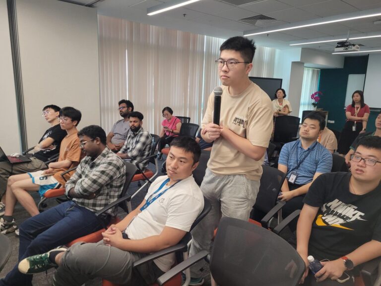
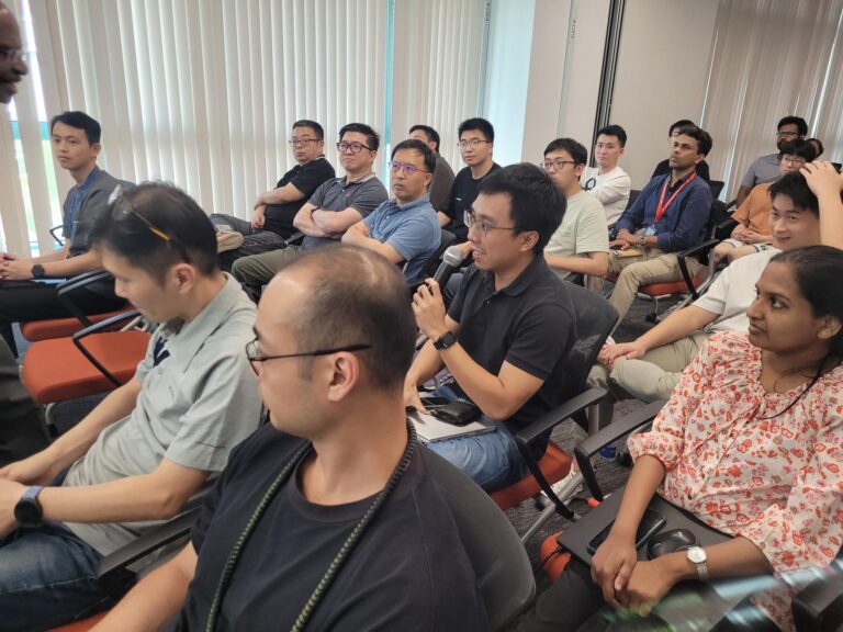
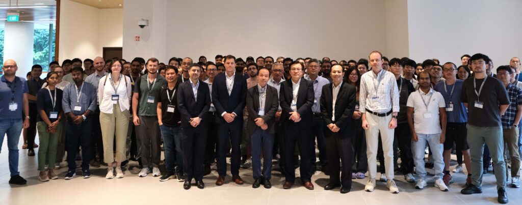
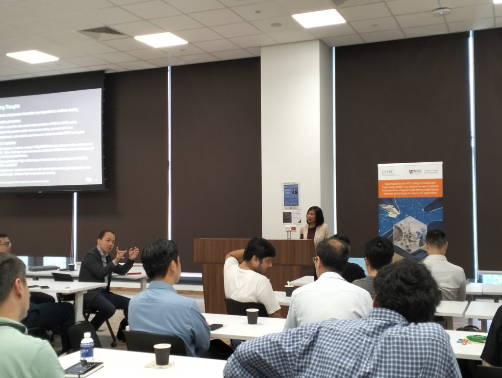
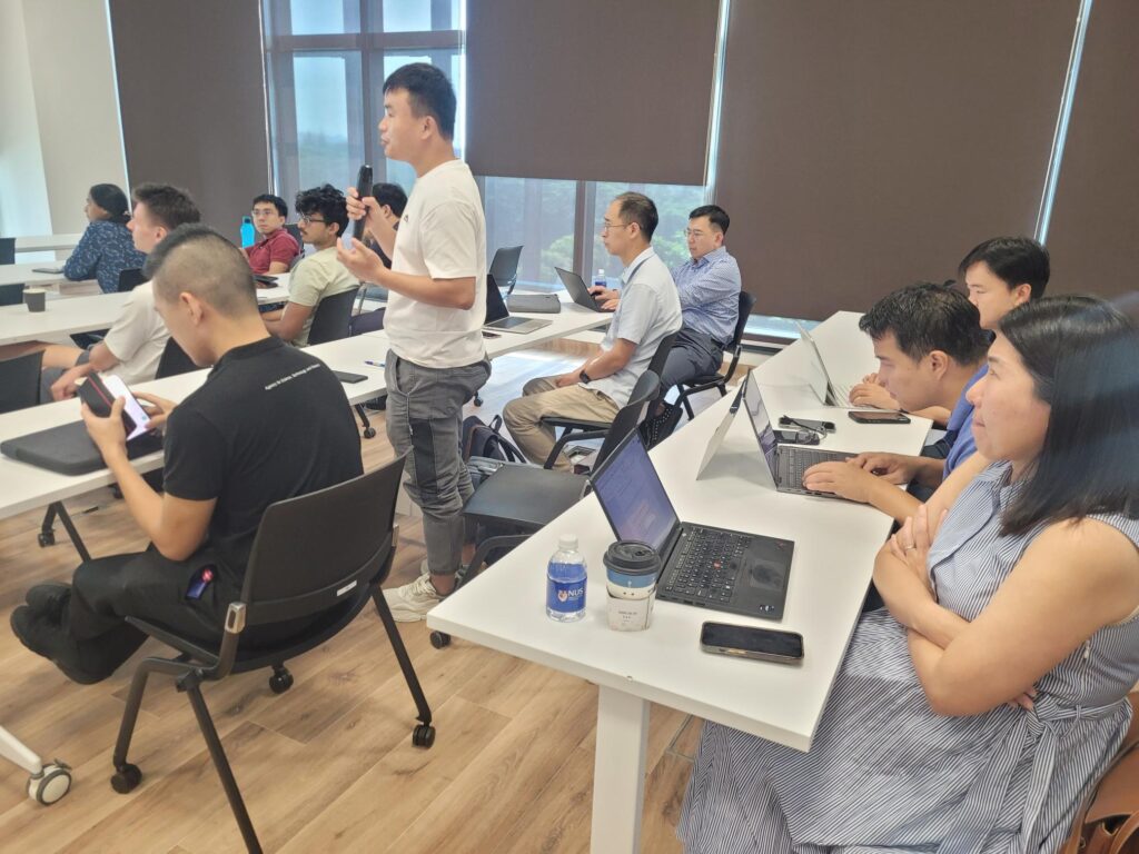
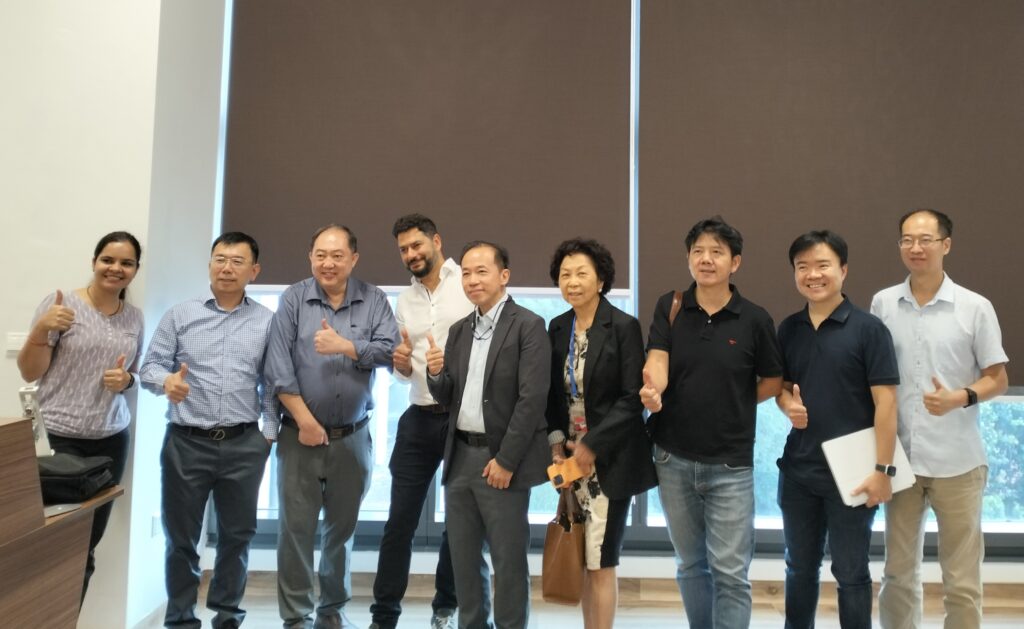
The SHINE 5th Technical Workshop was held on October 3, 2024, at the NUS E7 Building, Level 3 Seminar Rooms. The event focused on advancing packaging technologies, hybrid electronics, and innovative materials, while addressing industry trends and challenges to promote co-development collaborations. The workshop attracted a diverse audience of professors, staff, researchers, and industry collaborators, contributing to its success.
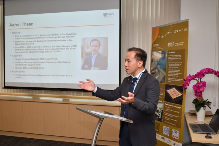
Professor Aaron Thean, Director of SHINE, opened the workshop with a welcoming address, emphasizing SHINE’s vision to tackle challenges in hybrid integration through its focus on packaging technologies and hybrid electronics. He shared highlights of SHINE’s current work packages and provided a glimpse into the afternoon session, which would include the presentation of a novel BEOL device architecture for 3D memory and an ultra-sensitive, flexible printed resistive strain sensor designed for harsh environments—both of which are featured in a recent SHINE paper accepted by IEDM.
Three distinguished industry speakers were featured during the event:
Mr. Kam Lee, Senior Director and Design Head of Advanced Packaging Technology and Service at TSMC, presented TSMC’s product roadmap for advanced packaging. He illustrated how performance scaling is being extended through system integration, driven by AI mega trends and High-Performance Computing (HPC) demands. He emphasized TSMC’s pivotal role in enabling chiplets through advanced packaging and testing technologies to meet these performance demands.
Mr. Jared Holzwarth, Vice President of Technology at AIXTRON SE, delivered an insightful talk on AIXTRON’s leadership in Metal-Organic Chemical Vapor Deposition (MOCVD) technology. He emphasized how controlling volume production of low-cost compound materials opens new opportunities for the semiconductor market. Mr. Holzwarth outlined AIXTRON’s journey from small reactors to fully automated systems, enabling scalable production without compromising quality or cost, and described how AIXTRON has facilitated the transition of materials from research to high-volume manufacturing.
Mr. Samir Mowla, Vice President of Corporate Development at AEM, discussed the primary challenges in semiconductor device testing, especially in light of HPC, AI, and mobile communication advancements. He highlighted innovative testing methodologies, including solutions for thermal spikes, and explored how companies are maintaining product quality while managing cost-effectiveness in an increasingly complex and competitive landscape.
The morning sessions concluded with Prof. Lim, who provided an overview of SHINE’s research activities and highlighted the centre’s focus on new material innovations and flexible electronics. He encouraged continued collaboration with SHINE to drive future advancements in hybrid electronics.
For SHINE consortium members only, the afternoon workshop featured a total of 9 professors and researchers from NUS, NTU, University of Berkely, California from Thrust 1 to Thrust 4, and A*Star, who share their respective research works and highlights.
Flexible Antenna System: Thermal Management and Integration Challenges by NUS Senior Research Fellow, Dr Evgeny Zamburg, SHINE Thrust 3.
Design and Preparation of Printable Inks for Thermal Management and Energy Harvesting by NTU Senior Research Fellow, Dr Hyunwoo Bark, SHINE Thrust 2.
Manufacturing Roadmap of Flexible Hybrid Electronics by NTU Professor, Chen Xiaodong, SHINE Thrust 2, Co-Investigator and SHINE Deputy Director.
NUS presented ‘Innovative Flexible Antennas for Conformable Phased Arrays’ by NUS Professor, Koen Mouthaan, SHINE Thrust 3, Co-Investigator.
Design of Through Silicon Interposer for 2.5D Heterogeneous Integration for High-mix Application: From Wafer to Functional Packaging by A*Star IME Scientist, Dr Zhou Lin.
Semiconducting Single-walled Carbon Nanotube Thin Film Transistor (sSWCNT-TFT) via Jet Nebulizer Spray Pyrolysis (JNSP) by NUS Research Fellow, Dr Murugan Balaji, SHINE Thrust 4.
Hierarchical Bound States and Anderson Phases in Topological Heat Transport’ by NUS PhD Student, Mr Yang Shui Hua, SHINE Thrust 4.
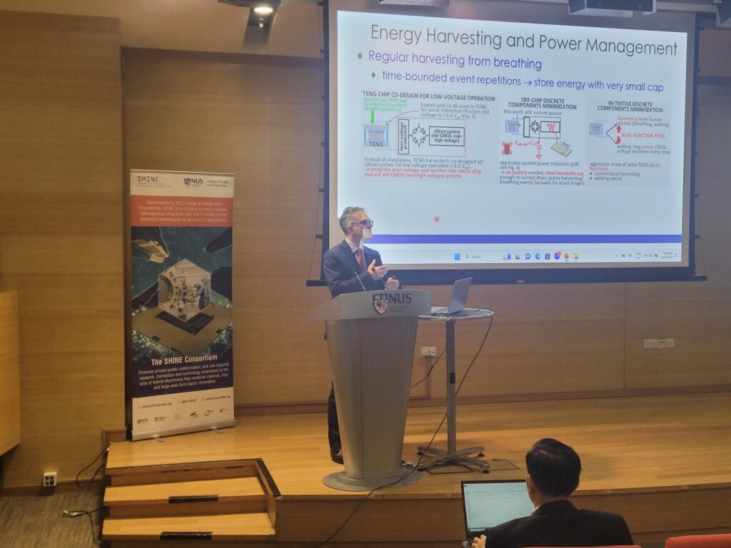
Pushing SHINE Innovation to a Complete Ultra-Low Power Chiplet Ecosystem with Silicon Demonstrations by NUS Professor, Massimo Alioto, SHINE Thrust 1.
From Automated Design to Heterogeneous Integrated Electronics by University of California, Berkeley USA Professor, Alberto Sangiovanni- Vincentelli, SHINE Thrust 1, Research Collaborator.
In conclusion, the SHINE 5th Technical Workshop was an invaluable opportunity for attendees to gain insights into cutting-edge technology developments in advanced packaging, testing, and materials development, all essential to addressing the evolving needs of the semiconductor industry.
Event Gallery
Material Innovation in the Atomic Scale Era – An Industry Perspective September 23, 2024
Material Innovation in the Atomic Scale Era – An Industry Perspective
Date: 23 Sep 2024
Time: 10.30 am to 11.30 am
Venue: Blk E7 Seminar Room 4
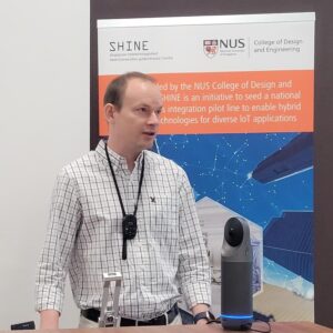
On 23 September 2024, SHINE had the privilege of hosting Dr. Dina Triyoso from TEL Technology Centre, USA, for a seminar titled “Material Innovation in the Atomic Scale Era – An Industry Perspective.”
Dr. Dina Triyoso underscored the indispensable role of material and process innovation in the continued scaling of semiconductor technologies. She elaborated on the effectiveness of selective processes, such as the studied implementations of Atomic Layer Deposition (ASD) for CMOS scaling, and highlighted how a selective Ruthenium process is key for future interconnect scaling. Dr. Triyoso pointed out that after many decades, advancements in high-k materials, notably the transition from silicon dioxide to hafnium-based high-k dielectrics, are pivotal for deploying high-k metal gate applications in planar technology and fully depleted devices. The future applications of high-k materials, focusing on their ferroelectric properties, include Ferroelectric RAM (FeRAM) and Negative Capacitance Field-Effect Transistors (NCFET).
In closing, Dr. Triyoso emphasized that as the semiconductor industry progresses, material innovation becomes increasingly vital. Key areas of focus include precise grain control, maintaining optimal material properties under low thermal budgets, and ensuring resilience to high-temperature processing. Looking ahead, the industry researchers will continue to prioritize refining these processes and materials to meet evolving technological demands. The attendees undoubtedly gained a lot from Dr. Dina’s deep industry insights, which sparked many questions from the floor. We extend our sincere appreciation to Dr. Dina Triyoso for her enlightening presentation and look forward to more thought-provoking discussions on the future of semiconductor technology.
Speaker Biography
Dr Dina Triyoso is a Technologist & Senior Member of Technical Staff at TEL Technology Center, America, LLC. She received her PhD in Chemical Engineering from Texas A&M University. Prior to joining Tokyo Electron in 2019, she spent 18 years at Motorola/Freescale and GLOBALFOUNDRIES working on process and integration of new materials in CMOS (planar, FINFET and FDSOI). Her current research is focused on new materials and new process technologies for future logic and memory devices. Dr Dina has 37 issued US patents and over 150 publications. She is the 2023 IEDM General Chair and the Associate Editor for IEEE Transactions on Electron Devices.
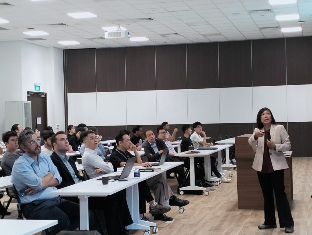
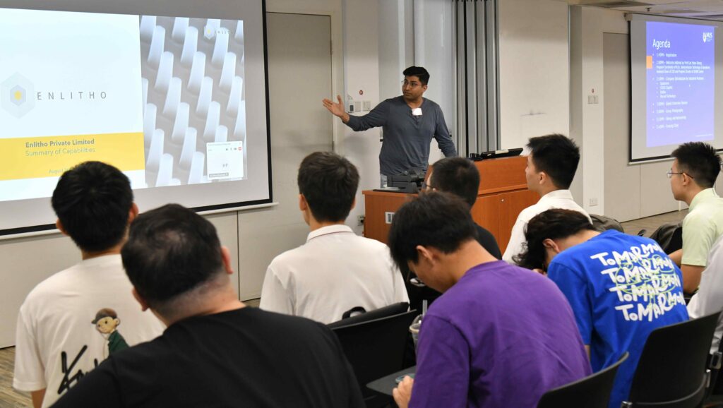
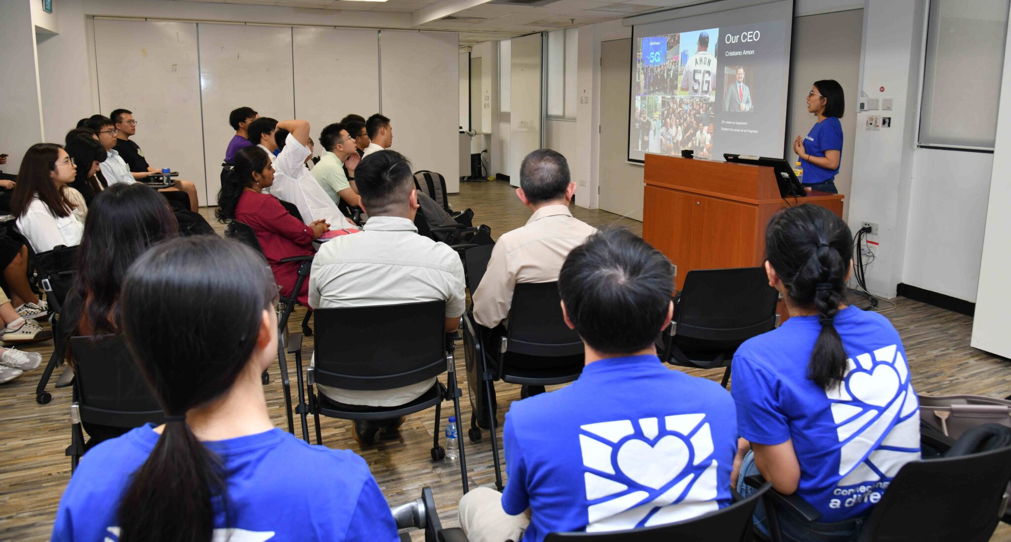
MSc STO, Internship Day September 9, 2024
MSc STO, Internship Day | 9 Sept 2024
Date: 9 Sept 2024, Monday
Venue: NUS, CDE E4 Building
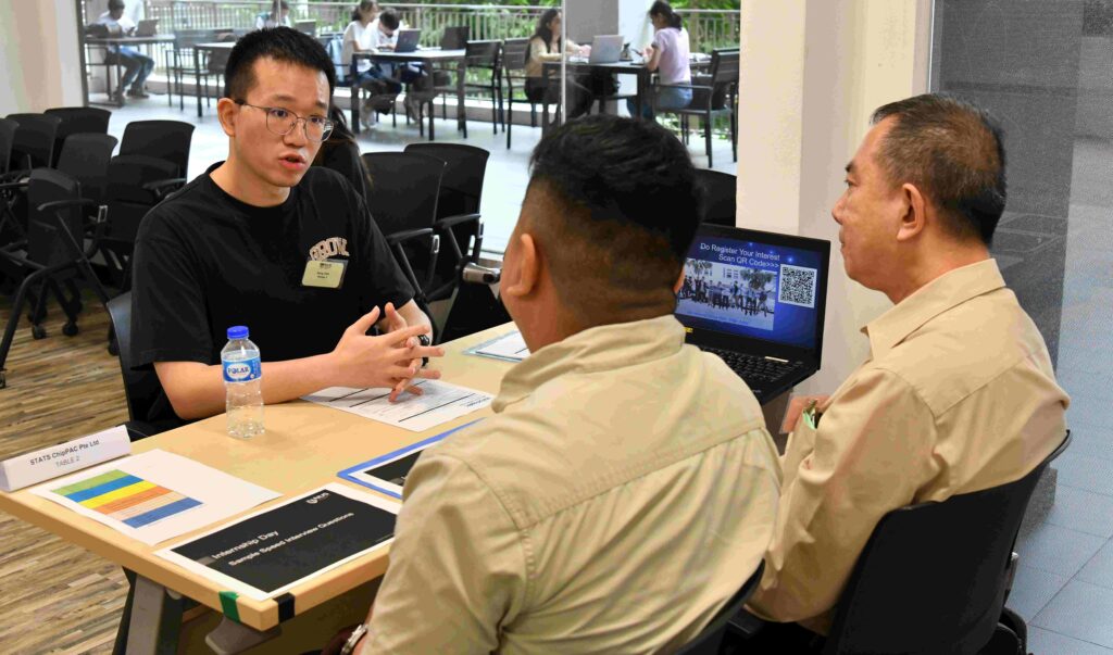
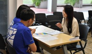
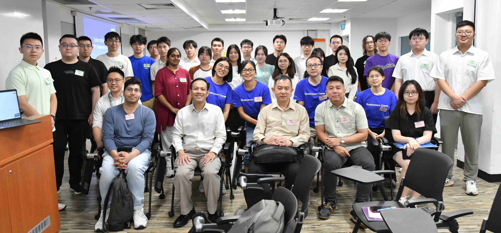
On 9 September 2024, SHINE had the privilege of inviting and hosting industry representatives from Enlitho, Marvell, Qualcomm, and STATS ChipPAC for the Internship Day for the inaugural cohort of the Master of Science in Semiconductor Technology and Operations (MSc STO) programme.
The insightful presentations gave students a deeper understanding of the vast opportunities within the semiconductor industry, while the speed interview sessions conducted by the participating companies significantly enhanced their chances of securing internships.
We sincerely appreciate the contributions of all involved, from the company representatives to the NUS support staff, whose efforts ensured the smooth execution of the event and positive outcomes for the MSc STO program.
Guest Lecture for MSc STO September 2, 2024
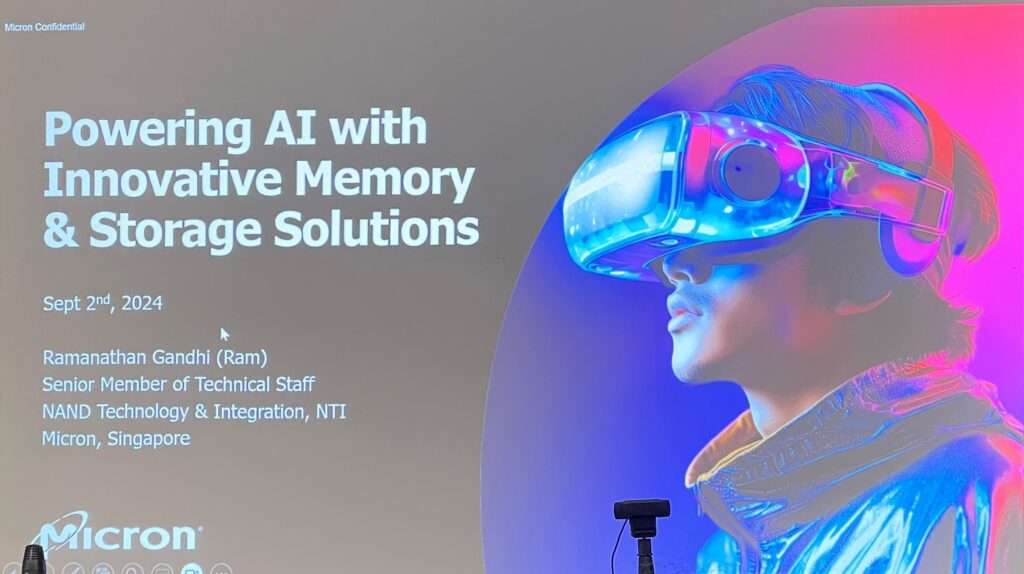
Guest Lecture for MSc STO – Powering AI with Innovative Memory & Storage Solutions
Date: 2 Sept 2024, Monday
Time: 6 pm to 8 pm
Venue: NUS, CDE EA Building
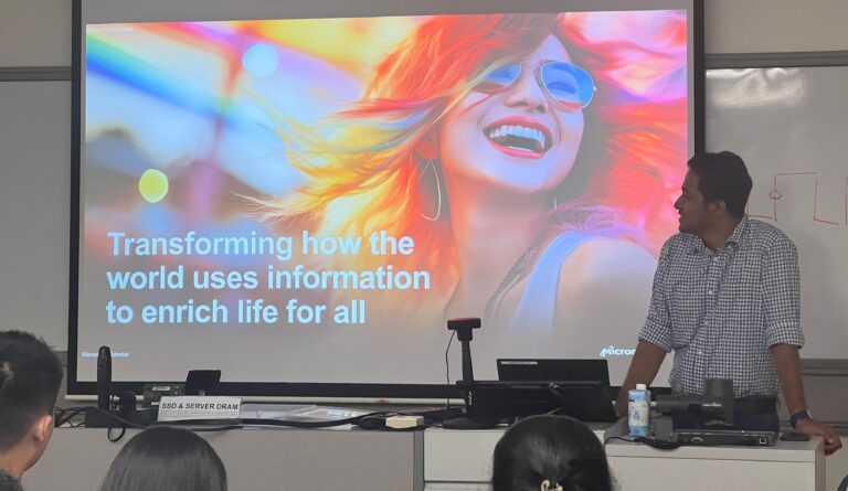
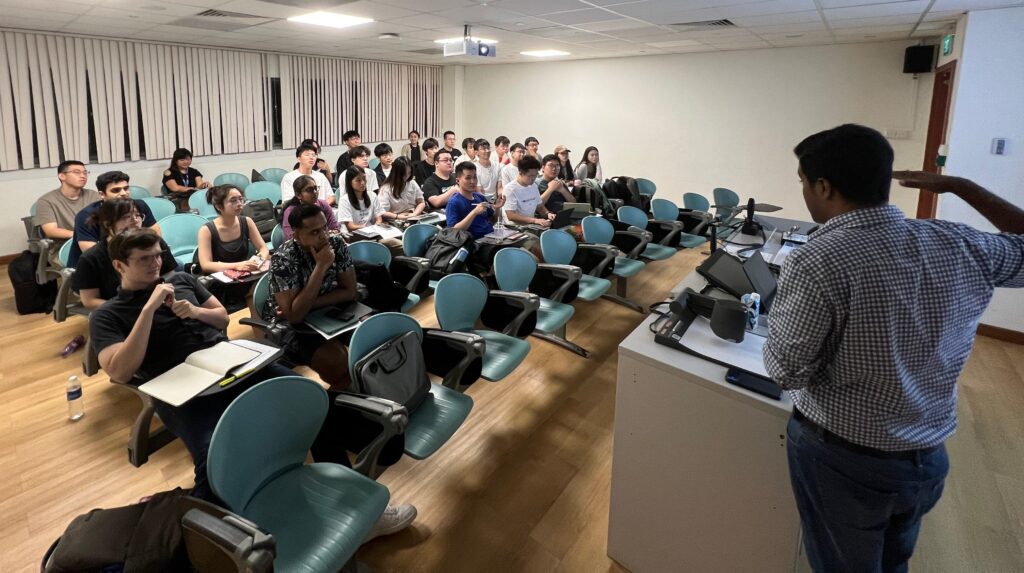
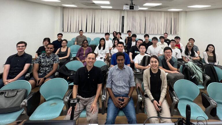
SHINE was honoured to welcome Mr. Ramanathan Gandhi (Ram) from Micron Technology for his illuminating guest lecture on ‘Memory & Storage Landscape and Its Role in AI,’ delivered to our MSc Semiconductor Technology and Operations students on 2 September 2024
Mr. Ramanathan’s lecture offered transformative insights, equipping our students with invaluable knowledge on key topics such as HBM, SSDs, and memory architecture. His ability to demystify complex subjects left a lasting impression on the audience, and it was encouraging to witness active student participation and meaningful discussions with him.
The session’s key highlights included an introduction to Micron Technology, an overview of memory architecture and landscape, and an in-depth exploration of memory and storage’s critical role in AI’s advancement. The lecture not only ignited thought-provoking discussions but also provided significant industry insights, effectively bridging the gap between academic studies and practical applications.
We are profoundly grateful to Mr. Ramanathan for delivering such an enriching experience and to Ms. Glenda Chong of Micron Technology for facilitating the guest speaker. We eagerly anticipate more industry-sharing sessions with Micron Technology, as we work together to develop talent for the betterment of society in the era of AI.
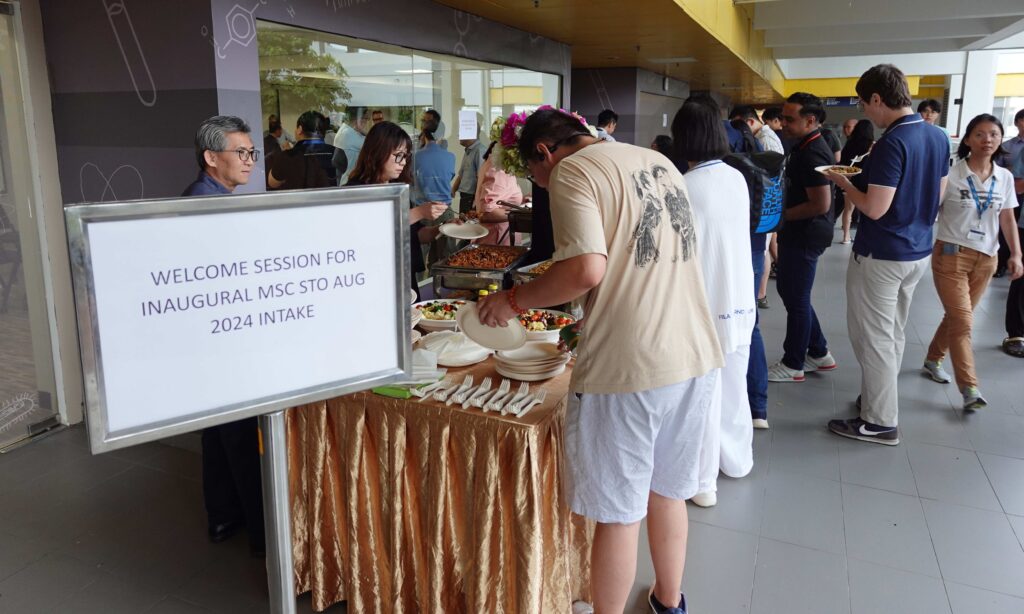
Welcome Tea Reception for the Inaugural MSc STO Aug 2024 Intake August 12, 2024
Welcome Tea Reception for the Inaugural MSc STO Aug 2024 Intake
Date: 12 August 2024, Monday
Time: 4 pm to 6 pm
Venue: NUS, CDE E4 Building, E-Cube
On 12 August 2024, SHINE had the pleasure of playing a part in the welcoming tea reception at E-Cube seminar rooms within the campus of the NUS College of Design and Engineering for the first cohort of students for the Master of Science in Semiconductor Technology and Operations (MSc STO) program. Hosted by the NUS Department of Electrical and Computer Engineering (ECE) in collaboration with the Department of Industrial Systems Engineering and Management (ISEM), the Department of Materials Science and Engineering (MSE), and SHINE, the event was enthusiastically attended by the students, professors, lecturers, and staff.
The event commenced with a welcome address by Prof. Aaron Thean, Provost of NUS and Director of SHINE, who provided an overview of current developments in the semiconductor industry. He highlighted the industry’s multidisciplinary scope, encompassing basic sciences such as physics and chemistry, as well as engineering and business. Prof. Thean concluded by offering his best wishes to the new students as they embark on their academic journey.
Prof. Biplab Sikdar, Head of the NUS Department of ECE, followed with an inspiring speech about the structure of the MSc STO program. He emphasized the importance of internships and projects as integral components of the curriculum, designed to equip students with practical, hands-on experience that will make them highly attractive to industry employers upon graduation.
The insights shared by both professors resonated strongly with the students and faculty, setting a positive tone for the exciting journey ahead.
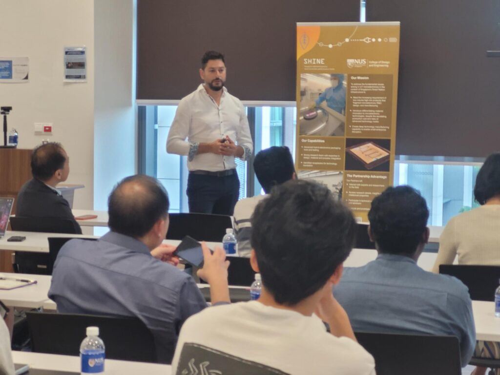
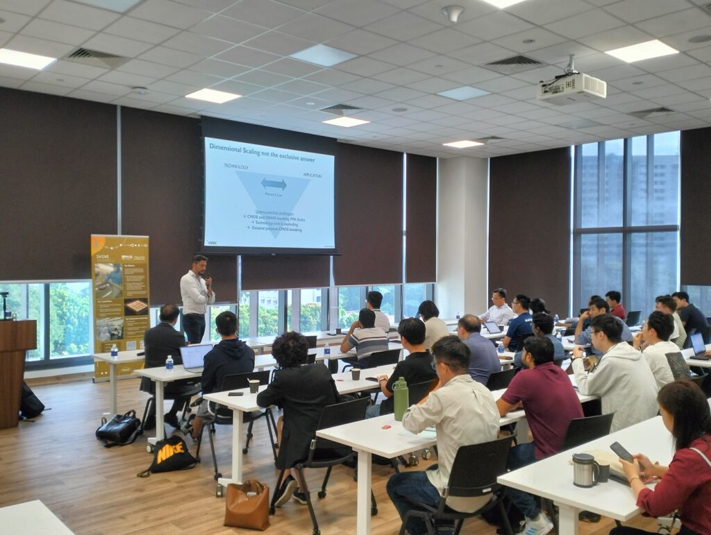
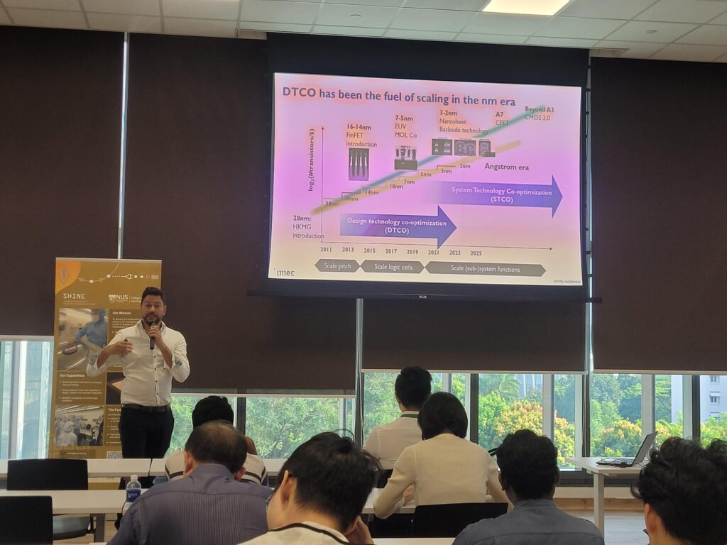
Talk on ‘Compute Scaling Beyond the finFET Era: The Road to CMOS 2.0’ July 15, 2024
Compute Scaling Beyond the finFET Era: The Road to CMOS 2.0
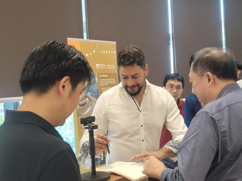
SHINE extends its heartfelt appreciation to Dr. Julien Ryckaert, Vice President of Logic Technologies at imec, for his visit to NUS and delivering a talk titled “Compute Scaling Beyond the finFET Era: The Road to CMOS 2.0” on 15 July 2024.
Dr. Ryckaert shared that as we enter the nanosheet era, the semiconductor industry realizes that it will not be on a smooth scaling curve for CMOS. New device architectures, BEOL scaling boosters, backside technology, 3D partitioning, and heterogeneous integration will all be instrumental in shaping the future scaling roadmap.
At the end of the talk, Dr. Ryckaert emphasized that the diversity and scaling out of future compute systems require a holistic approach to scaling, driven by System-Technology Co-Optimization.
The audience showed considerable interest and enthusiasm, engaging in a lively exchange of questions both during and after the presentation.
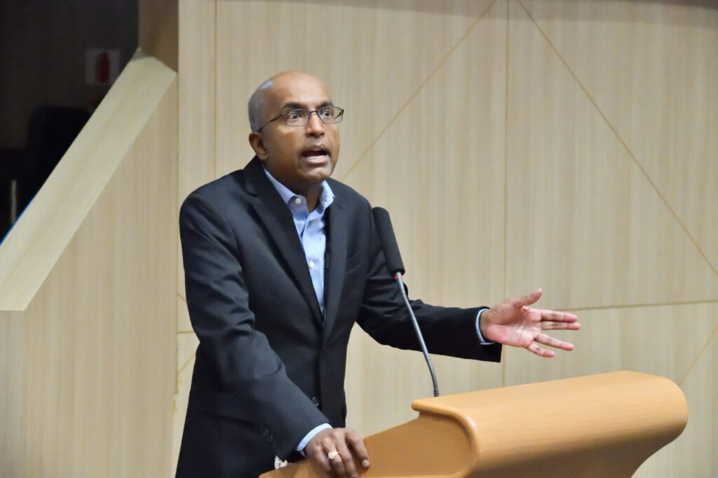
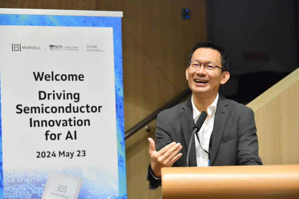
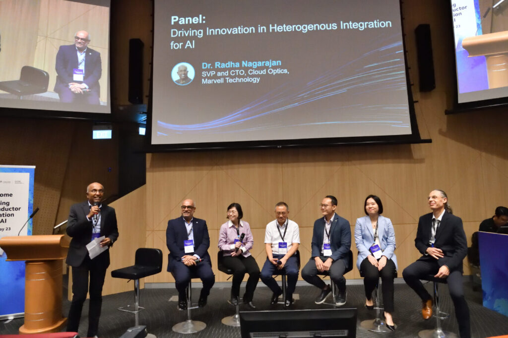
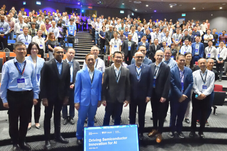
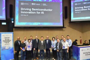
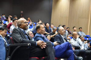
Driving Semiconductor Innovation for AI May 23, 2024
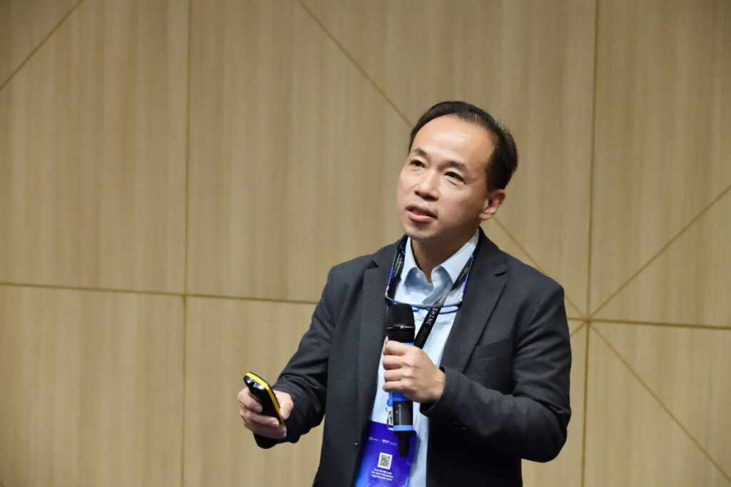
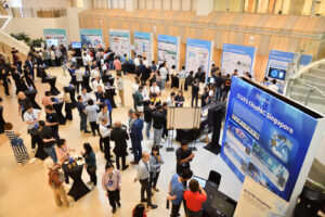
Led by Marvell, the joint event on Driving Semiconductor Innovation for AI by Marvell, NUS College of Design and Engineering and SHINE on 23 May 2024 was a resounding success, with about 350 attendees from diverse fields in engineering, computing, science and research across academia, research institutes and industry. Held at Block EA of the NUS College of Design and Engineering campus, the event featured a series of insightful sessions, engaging semiconductor ecosystem exhibition and memorable moments that left a lasting impact on all participants.
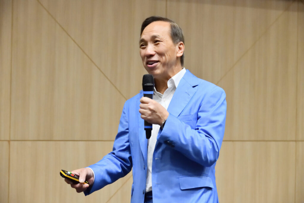
The event kicked off with a warm welcome from Dr. Radha Nagarajan, SVP and CTO of Marvell, setting the tone for the day, and preparing the audience of the exciting journey ahead on the development of integrated Circuit from Concept to Product at the exhibition floor.
The opening keynote by Mr Beh Kian Teck, CEO of NRF provided a glimpse of Singapore’s role in building a nation of entrepreneurs and innovators in semiconductor and AI. Singapore had moved from a nation of technician 40 years ago to a nation of entrepreneurs and innovators. To that note, we could find many parts in the gadgets that we own are manufactured in Singapore. Mr Beh indicated 3 pillars of innovation ecosystem that would move us one step closer to a nation of innovators and entrepreneurs. The first being the Science Base pillar which is fundamental to the growth of society where research is driven by curiosity. The second pillar being the Translation Engine under which the National Semiconductor Translation Centre serves to remove the high barrier of entry to start-up. The third pillar is to Build the Deep Tech Venture by bringing in ecosystem companies along with Deep Tech venture capital to co-invest in promising startup.
Mr Beh applauded the joint event by Marvell and NUS which helped to bring the community together. He said NRF is looking forward to Marvell, NUS and the larger group of people could continue to come together and organise the next integrated community event. He believes when the ecosystem lends their energy together, the community events become more integrated and is a lot more sustainable to engage the next generation of young people to the sector. In conclusion, Mr Beh said the promise of AI could only be sustainably realized if we succeed in pushing the boundaries of semiconductor innovation and Singapore hopes to contribute to this front by pushing the above mentioned 3 pillars of innovation ecosystem. He hopes today’s event is just the start to spark off the opportunity for partnership and collaboration.
The second keynote topic on Optical Interconnects for the AI Era by Dr Loi Nguyen revealed that Interconnects is a key enabling technology since the dawn of computing. The rapid growth of AI sees the need for optical interconnects enabling large AI Clusters. Dr Loi unveiled Silicone Photonics module for optical connects which convert electricity to light and vice versa. He was excited to share that majority of the chips optical interconnect are made by Marvell and Singapore is Marvell’s 3rd largest site outside of the US. He said this is the great times for semiconductor optics and engineers as they will be highly sought after. He announced the Marvell 6-month internship programme and invites NUS’ students to apply for the internship with the potential of them becoming a big family of Marvell when they graduated.
Prof Aaron Thean, Director of SHINE and Provost of NUS, delivered an insightful keynote on the topic of Heterogeneous Integration and the New Opportunities for Novel Material-System Co-Design. Prof. Thean stressed that semiconductors are the cornerstone of the AI-driven future. The development of more powerful machines relies heavily on advancements in semiconductor technology and discussed the recent and new trends of scaling evolution. He illustrated the progression of transistor scaling, showing a shift from geometric scaling to more complex, vertically stacked transistor configurations in modern 3D IC systems. He also noted a shift of the packaging technology from back-end to the front-end by packaging he chips and wire them together. He emphasized the necessity of integrating new materials, devices, and architectures to drive the innovation of heterogeneous 2.5D and 3D integrated circuits (ICs), and exciting new STCO (System Technology Co-Optimization) and DTCO (Design Technology Co-Optimization) are needed in achieving these innovations.
Prof. Thean moved on to introduce state of the art packaging facility at SHINE centre that bring together front-end online material innovation with advanced packaging capability. He said the centre allows students to have access to these huge tools to perform wafer level projects leveraging on advanced soldering capability, low temperature soldering and advanced die wafer. He emphasized that passion is needed for the research field and that the path forward to solving the problems of computing will not rely on a single process or approach. Instead, it must be a co-optimization of multiple technologies and strategies.
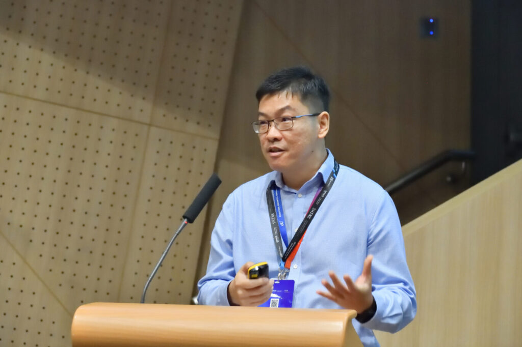
The last keynote speaker was Dr Terence Gan who delivered the topic on Enabling Research and Heterogeneous Integration in Singapore. Dr Terence Gan started off by thanking NRF for enabling A*Star IME with 8000 square meters of semiconductor cleanroom. He then walked the audience through the 10-year key milestone of Advanced Packaging Innovations at IME. He stated advanced packaging, as described, is heterogeneous, offering multiple integration possibilities beyond traditional methods. This includes options like CoWAS, high-density RDL with nano-packaging, and hybrid interposers combining photonics and electronics. A*Star IME positions itself as a one-stop-shop for tailored solutions, collaborating with partners including SHINE Centre to address diverse system requirements and offering translational research to facilitate industry grade low volume production. He concluded the talk by introducing the key team members, inviting engagement to turn ideas into reality through partnerships with SHINE, academia and industry scientists.
Panel Discussion:
Moderated by Dr Radha Nagarajan, a lively panel discussion on Driving Innovation in Heterogeneous Integration in AI featuring 6 panellists who shared their diverse perspectives sparked a thought-provoking conversation that resonated with the audience.
The panellists comprise Dr Arvind Sundarrajan, Managing Director, Applied Packaging Development Center and Singapore Semiconductor Products Group of Applied Materials; Dr Soh Yun Siah, VP, Technology Development of Singapore GlobalFoundries; Dr. Patrick Lo Guo-Qiang, CTO of Advanced Micro Foundry; Dr Alfred Yeo Swain Hong, Director, Research and Development of StatsChipPAC; Dr Chen Lan, Director, Product Development of AMD; and Dr Noam Mizrahi, EVP, Corporate Chief Technology Officer of Marvell.
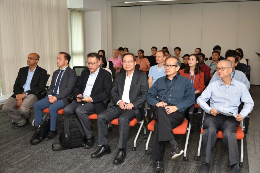
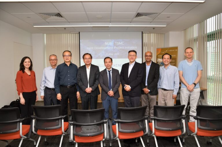
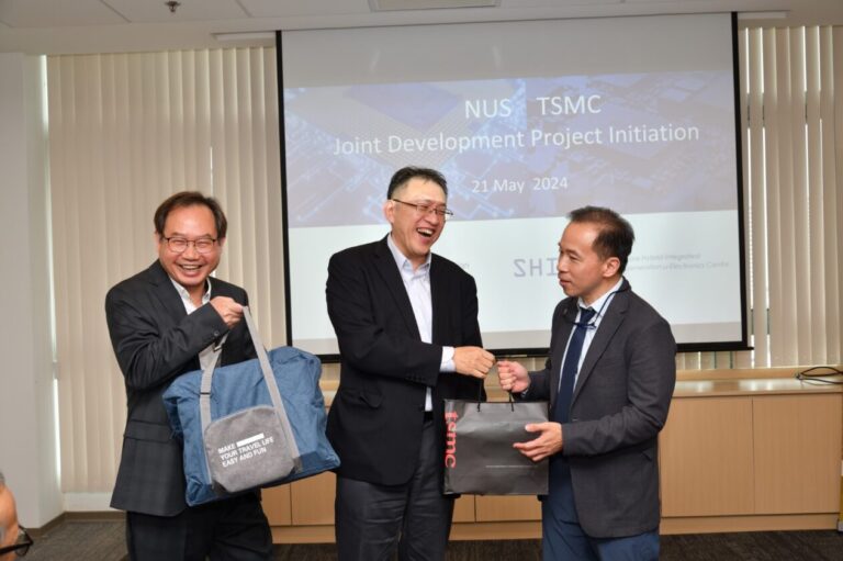
TSMC Visit to SHINE Centre | 21 May 2024 May 21, 2024
TSMC Visit to SHINE Centre | 21 May 2024
On 21 May 2024, SHINE, supported by the College of Design and Engineering, was honoured to host Dr. Marvin Chang, TSMC Director of University Programmes, Corporate Research, along with Dr. Chuei-Tang Wang, TSMC Technical Director of Advanced Packaging Technology (APTS) and Service, for an informal sharing session at NUS. This event marked the initiation of a collaborative project between TSMC and SHINE. Approximately 46 attendees, including SHINE management, the Head of the ECE Department, PhD students, and researchers, participated in the session.
In his welcome address, Prof. Aaron Thean, Director of SHINE and Vice President (Academic Affairs) and Provost of NUS, highlighted the significance of talent development for both NUS, a leading university, and TSMC, a major global semiconductor manufacturer. Prof. Thean extended an invitation to the TSMC scientists to consider joint professorship appointments at NUS, emphasizing the mutual benefits and collaborative opportunities between the institutions.
Following the welcome speech, Dr. Marvin Chang expressed the company’s enthusiasm to recruit talent from NUS, emphasizing the importance of joint talent development efforts.
Dr. Chuei-Tang Wang (CT Wang) shared his experiences, noting that his first visit to Singapore was over 15 years ago and this was his third visit. Since joining TSMC in 2022, Dr. Wang has been involved in the packaging research works. Some of his significant contributions include 170 US patents and 35 papers in prestigious conferences such as VLSI, IEDM, and ECTC. Dr. CT Wang announced that TSMC would sponsor two projects: the Advanced Freeform Optical Waveguide, led by Prof. Yeow Kheng Lim, SHINE Programme Director, and the Thermal Management Solution for High-power Wafer, led by Prof. Aaron Thean, SHINE Director, with Assistant Prof. Sunmi Shin of the NUS Mechanical Engineering Department as Co-investigator. He emphasized the importance of low power consumption chips and optical computing in the AI era, highlighting these as critical research areas.
Dr. CT Wang also shared insights into TSMC’s global presence, with over 760,000 employees across three continents and nine countries, including 12-inch Fab plants in Taiwan, Japan, China, and Singapore. He invited NUS students to join TSMC’s internship programs and explore career opportunities within the company.
The event proceeded with a group photo and a heartwarming gift exchange between Prof. Aaron Thean, Dr. Marvin Chang and Dr. CT Wang, representing NUS and TSMC, respectively.
Following this, Prof. Yeow Kheng Lim provided an overview of the SHINE Centre, emphasizing its focus on hybrid integration and hybrid electronics. He highlighted SHINE’s commitment to driving disruptive innovation, enabling academia-industry co-research, and incubating small-scale spin-offs through collaboration with industrial partners.
Prof. Lim also introduced the recently launched Master of Science in Semiconductor and Technology Operations, further demonstrating SHINE’s dedication to talent development in partnership with the semiconductor manufacturers and players.
Dr. Evgeny Zamburg concluded the sharing session with a detailed presentation of the group’s research on Thermal Management Solutions, a project done in collaboration with A*Star and Soitec. The research involved innovative approaches to heat spreading, absorption, and radiation materials, resulting in a cost-effective 8-inch wafer-compatible interposer.
At the end of the session, Prof. Aaron Thean and Prof. Yeow Kheng Lim led Dr. Marvin Chang, Dr. CT Wang, and other TSMC representatives on a tour of SHINE’s cleanroom and dry lab facilities. The event concluded with a closed-door meeting to discuss technological challenges and brainstorm ideas for future research collaborations.
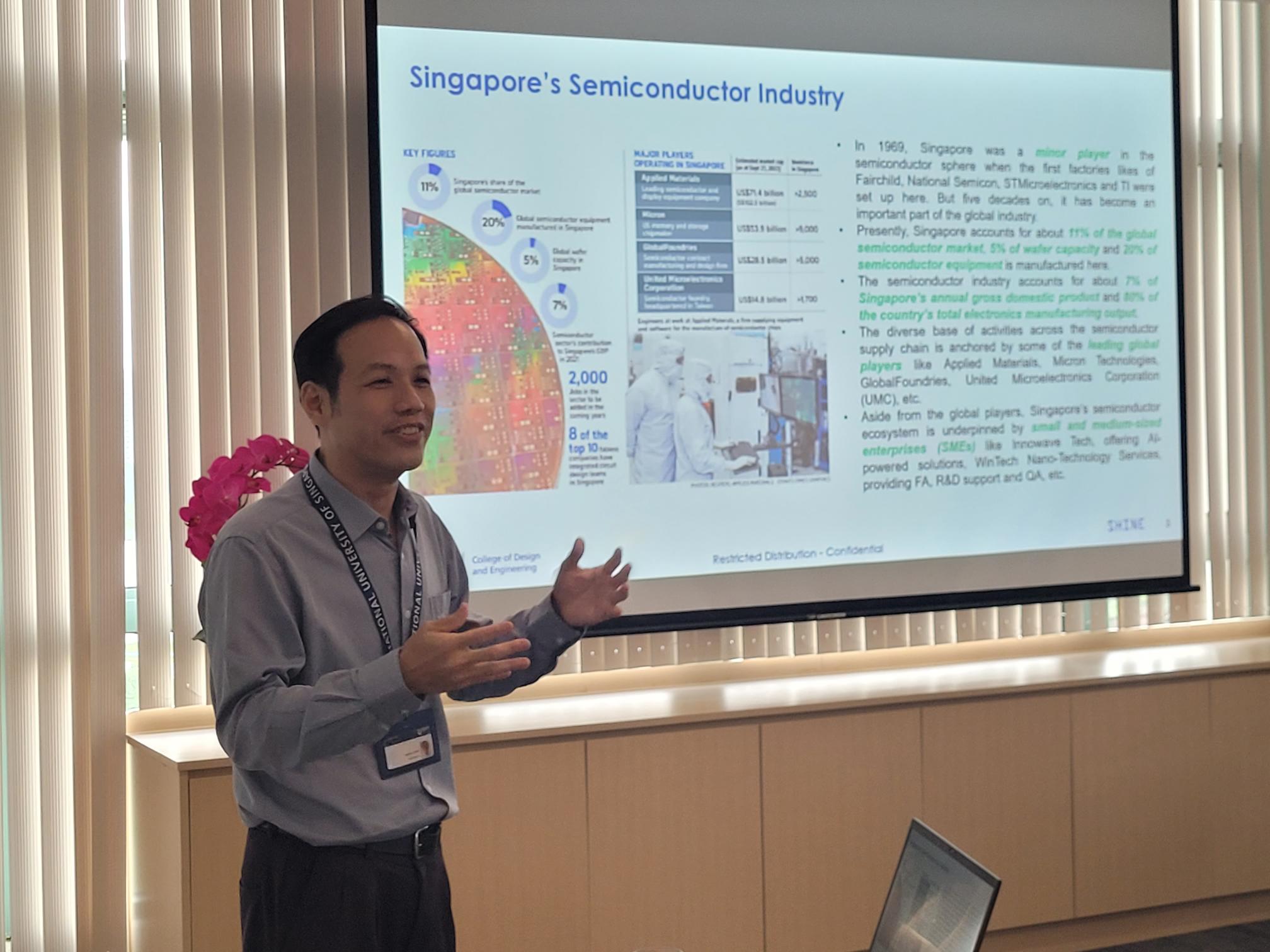
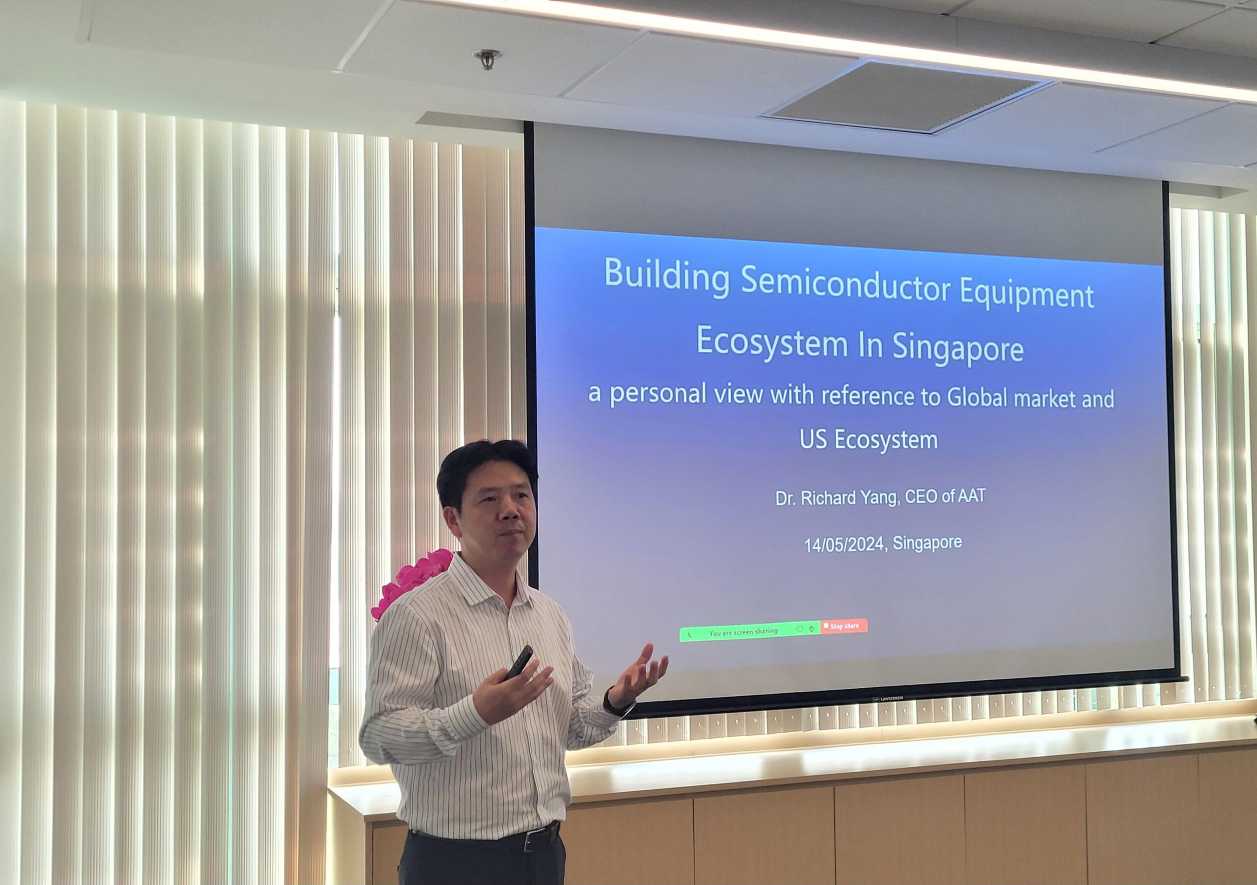
Building the Semiconductor Equipment Ecosystem in Singapore May 14, 2024
Post Event Report
Building the Semiconductor Equipment Ecosystem in Singapore
SHINE was honoured to be the co-host of the seminar organised by SHINE esteemed partner, Applied Angstrom Technology (AAT) titled “Building the Semiconductor Equipment Ecosystem in Singapore” which was held on 14 May 2024 at Block E6 of the NUS College of Design and Engineering campus.
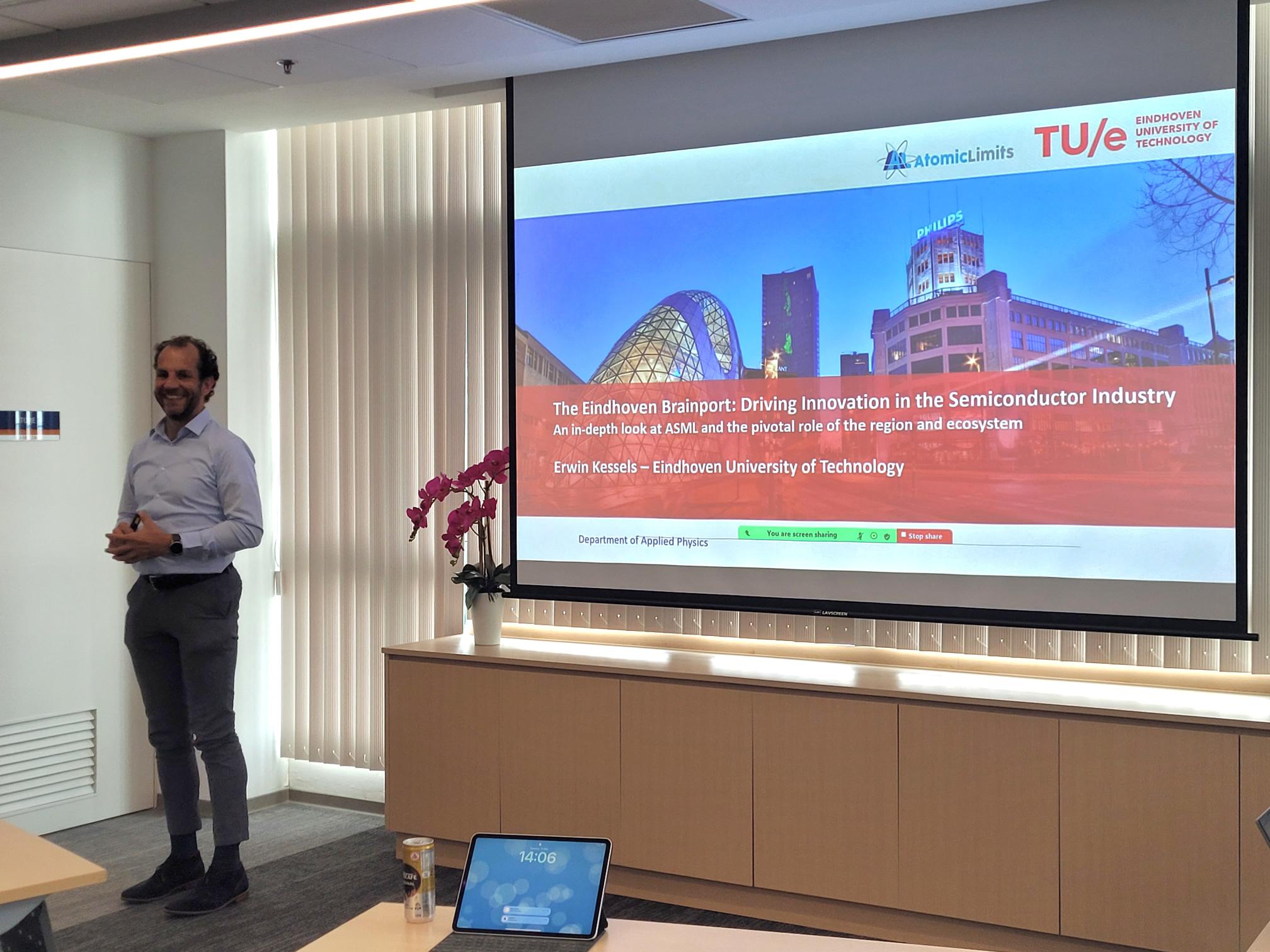
Prof. Erwin Kessel from Eindhoven University of Technology, Dr. Richard Yang, CEO of AAT, Prof. Lim Yeow Kheng, Programme Director of the SHINE Centre, and Mr. Michael Jin, Technology Innovator from Foothill Ventures were the speakers /panellists of the event.
The seminar covered critical topics such as the building of semiconductor ecosystems, infrastructure, talent development, the necessity of government support, and industry collaboration globally. The open discussion session sparked great interest in deep tech funding, highlighting its potential to help innovative startups gain traction, secure investment, and achieve growth.
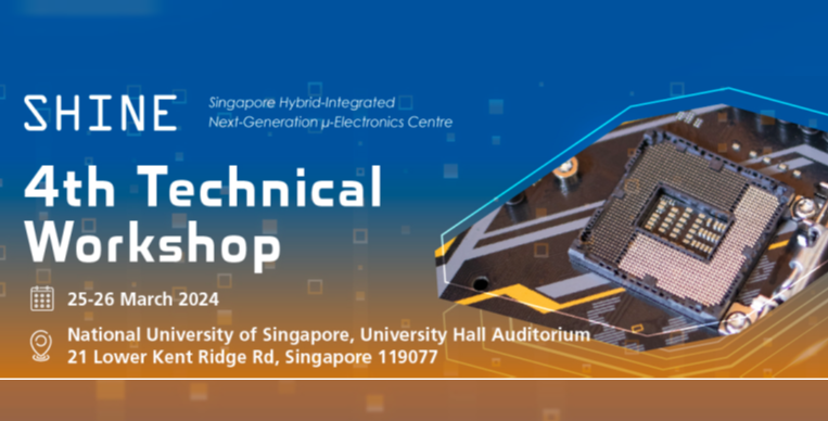
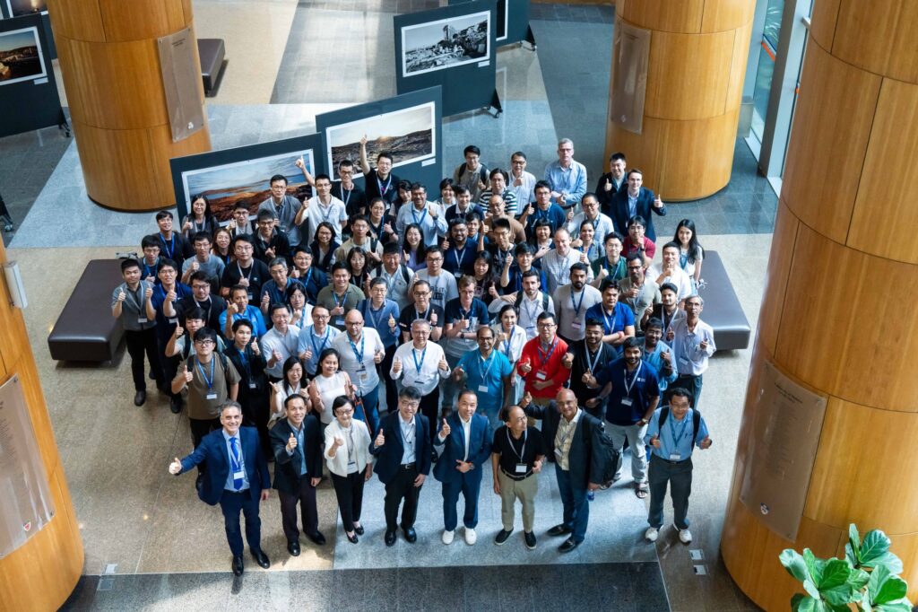
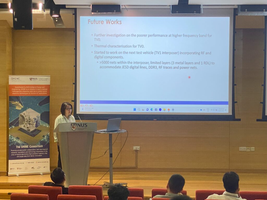
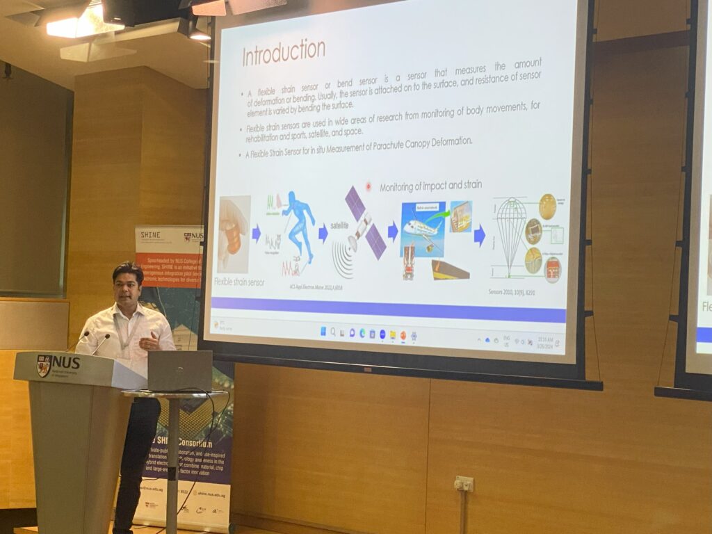
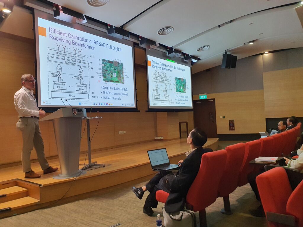
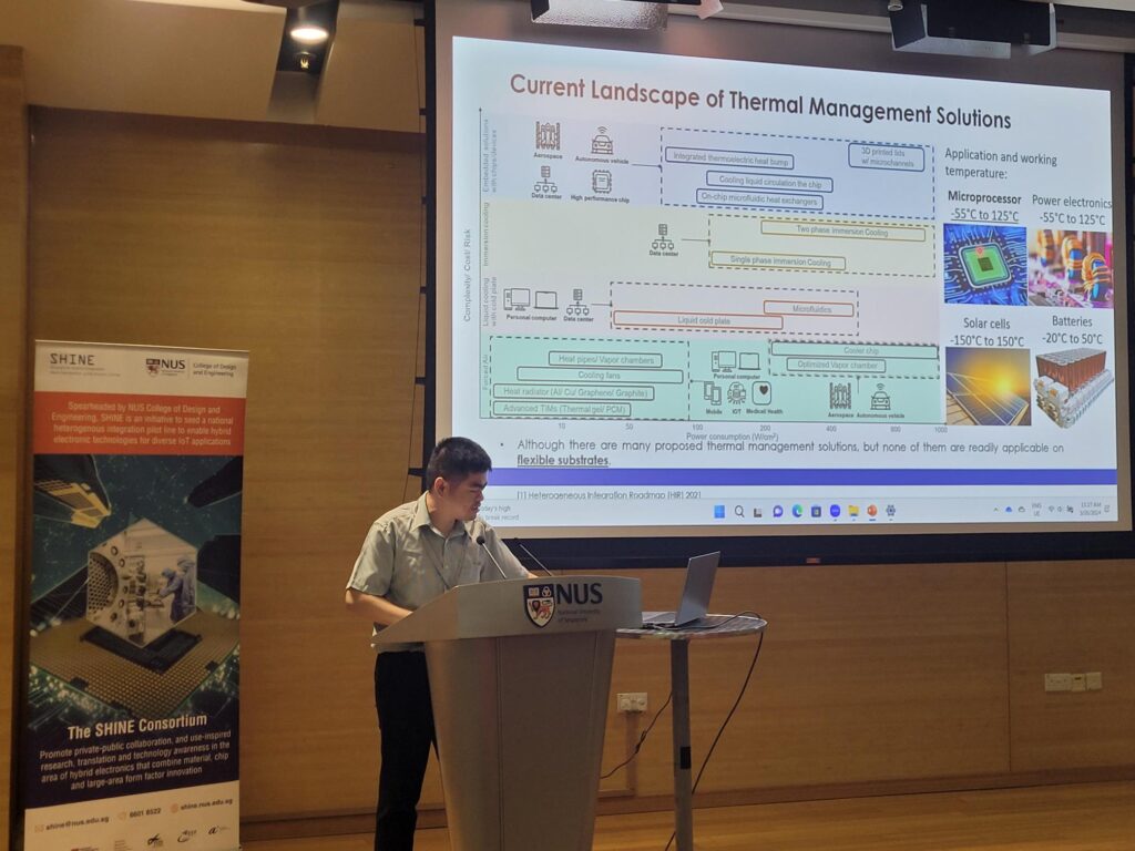
The 4th technical workshop of the Singapore Hybrid-Integrated Next-Generation μ-Electronics (SHINE) centre took place on 25th and 26th of March 2024, at the NUS Auditorium. The seminar focused on advancing new material discoveries for future semiconductor technology, defence electronics, photonics and device integration demonstrating innovation and innovative collaboration within the industry.
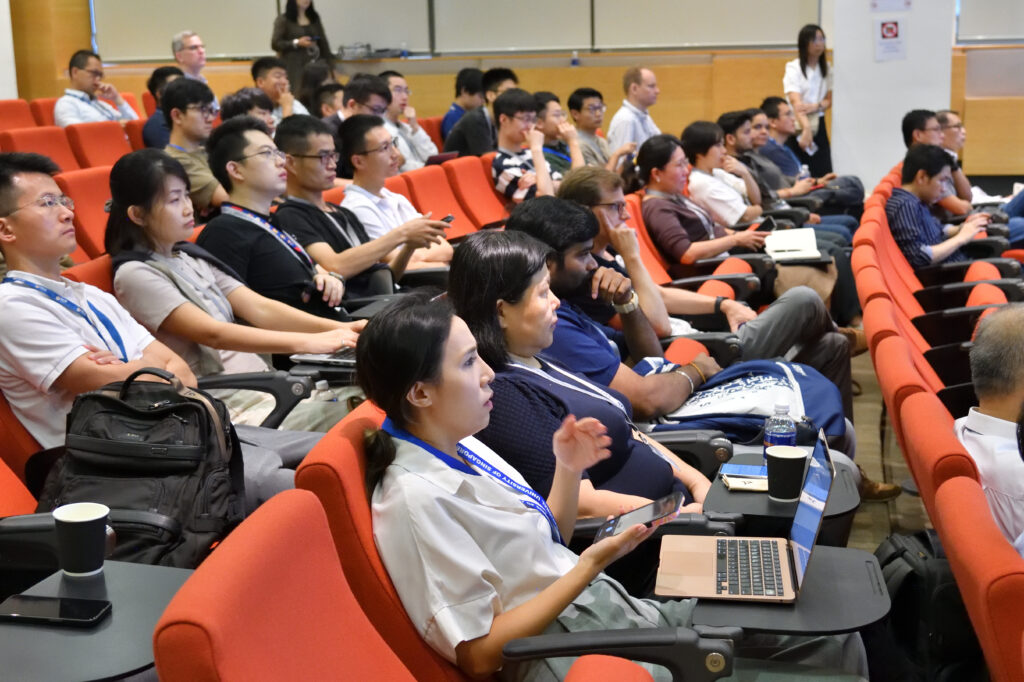
Day 1 of the event was open to the public, professors, staff, researchers, and industry collaborators, drawing in about 100+ participants both onsite and online.
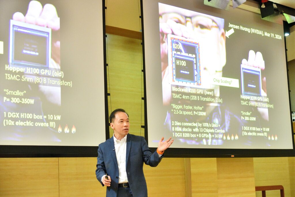
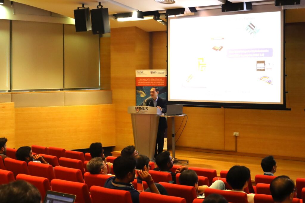
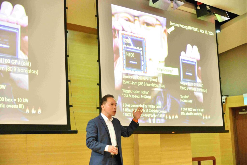
Professor Aaron Thean, Director of SHINE, commenced the conference with a welcoming speech. He shared the highlights from the recent Nvidia CEO Jensen Huang’s GTC keynote, featuring it as the future of everything. Jensen Huang, Nvidia launched on Mar 19, 2024, a “bigger, Faster, Hotter” with higher speed “2.5-5x speed, P=1200W with TSMC 4nm chip”. Prof Thean highlighted its alignment with SHINE from the new challenges as he articulated SHINE’s R&D Mission to enable interdisciplinary Innovations for Heterogenous & Hybrid Systems Integration that strives to solve the area of hybrid electronics where there has not been innovation in this area with a potential differentiation for many smaller players.
Citing some of SHINE’s innovations, including Stretchable low-resistivity interconnect systems. Prof Thean emphasized partnership and ecosystem building for translational heterogeneous electronics innovation nursery to drive disruptive innovation and translation,
enable acad-industry co-research sandbox, and incubate small-semi spin-offs and talent creation and development. He introduced SHINE’s shared facilities to spur capabilities akin to some of the industry’s standards and its diversity of talents. He reiterated the alignment of SHINE with the latest launch by Nvidia, bringing a new Era with exciting new opportunities going beyond Moore’s law.
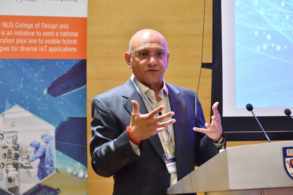
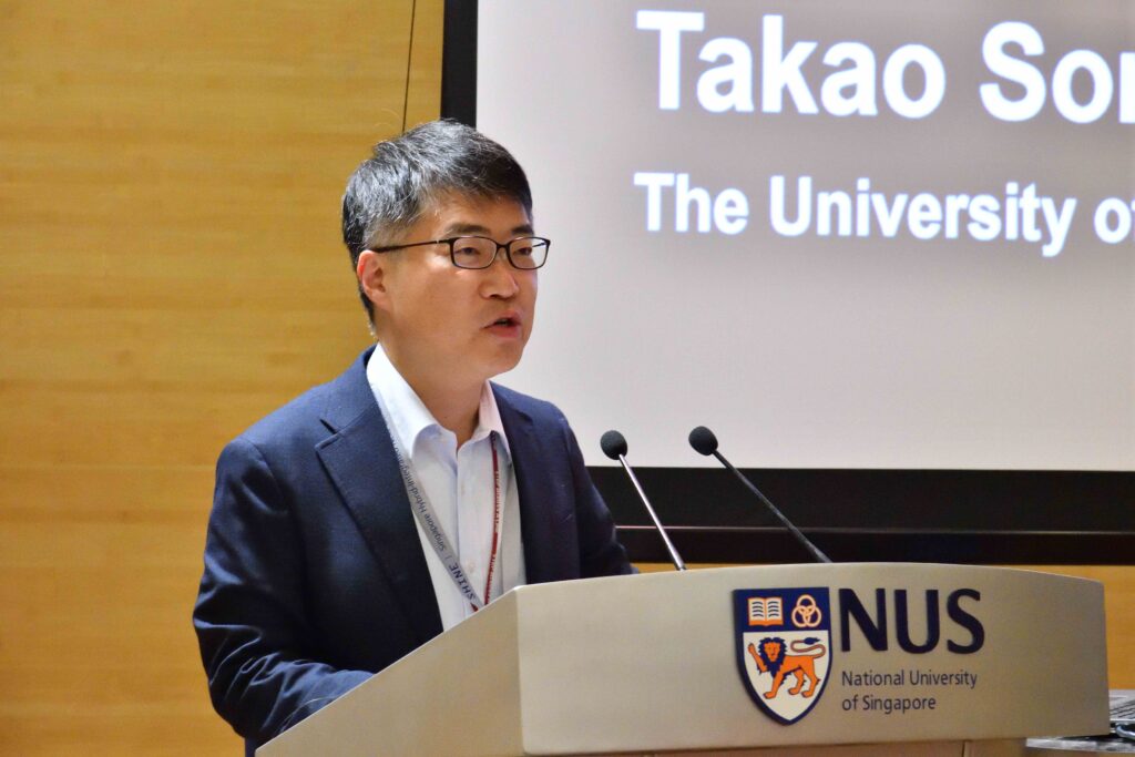
SHINE had the privilege of arranging five distinguished speakers, including Prof Philip Wong, Professor of Electrical Engineering Stanford University, USA; Dr Suresh Venkatesan, CEO of POET Technologies; Dr Vincent Leong, Director RF Programme DSO National Laboratories; Prof Takao Someya, Executive Director and Vice President (Start-up) & Professor, Graduate School of Engineering at The University of Tokyo; and Dr Guillaume Besnard, Research Engineer SOITEC.
The keynote address by Prof Philip Wong accentuated the significance of semiconductor advancements in future electronic systems, emphasizing the importance of three-dimensional integration. He introduced the concept of Nanosystems of 3D integrated “X” technology (N3XT) and underscored the need for MOSAIC integration to assemble chips into systems. In a nut shell, his discussion centred on developing new materials, device technologies, and design concepts for energy-efficient computing systems to achieve this vision.
Dr Vincent Leong, the third speaker of the seminar explored Trends in Defence Electronics, including miniaturization, pushing for higher RF power and leveraging commercial technologies, presenting insights into technology’s role, such as electronic warfare, on contemporary battlefields and forecasting its impact on defence electronics. He wrapped up his presentation by emphasizing the potential of research conducted at the SHINE research centre to propel these trends forward and foster innovation within the realm of defence electronics.
Next, Dr Suresh Venkatesan delved into Photonics Technologies for the next era of AI Computing and Data Center Interconnects. He featured the shift towards photon-based data transmission and processing, distinguishing it from traditional electron-based methods. The emergence of photonic fabrics presents new opportunities for AI workloads, particularly in deep learning applications like ChatGPT. Anticipating accelerated AI development, Dr Venkatesan explored the growing importance of “semiconductorizing” photonics in enhancing hardware capabilities and its future implications for AI-driven solutions.
Subsequently, Prof Takao Someya presented Ultra-flexible Organic Photonics, focusing on the versatility of flexible and thin photovoltaics in various applications, including powering wearable electronics and soft robots. Achieving remarkable bendability and lightweight properties by reducing the thickness to several micrometres was a key accomplishment. Emphasizing high efficiency and stability under ambient air conditions as crucial factors, Prof. Someya highlighted recent advancements in ultra-flexible organic photonics for next-generation wearables with novel applications of fully solution-processed PPG sensors and high-definition flexible imaging systems that will ultimately harmonize with humans.
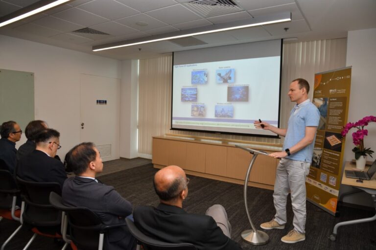
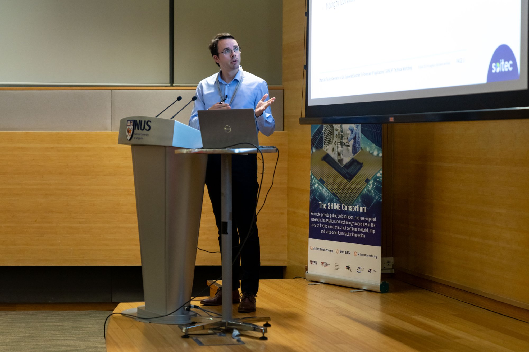
Dr Guillaume Besnard resumed after the lunch break with a presentation on SmartGaN, heralding it as the future of GaN-engineered substrates for power and RF applications. He underscored the increasing demand for semiconductors to power everyday devices and SOITEC’s commitment to engineering materials for enhanced performance and value at the system level, prioritizing energy efficiency and sustainability. He also shared industry concerns and paint points with GaN for power, such as price competition with silicon and RF applications like co-integration with CMOS. SmartGaN represents a pivotal advancement in this pursuit, leveraging SOITEC’s expertise in material science and Smart Cut™ technology alongside GaN epitaxy expertise. Additionally, Soitec is working towards for SmartGaN to become a solution to industry challenges, aiming a broader market acceptance for GaN, more open GaN device design and improved system value.
The series of invited talks concluded with Prof Lim featuring SHINE research activities and highlights. The open seminar ended at 2.55pm.
Throughout the event, there were eight stations of poster display featuring latest innovations and advanced technologies developed by the four SHINE research thrusts and industry partners such as AMD, POET Technologies and Soitec. This provided an avenue for engaging in technical discussions and exchanges among participants.
Eight presentations were delivered by SHINE research thrust co-investigators and research fellows during the two-day closed-door technical workshop, held from 3:00 pm to 5:00 pm on March 25th and from 8:30 am to 1:00 pm on March 26th.
In conclusion, the invited talks and technical workshops facilitated profound discussions among participants, nurturing collaborative dialogues and fostering essential knowledge exchange crucial for advancing the workshop’s objectives.
For further information about the speakers and synopsis of the talks and presentations, please download our event booklet.
The Photo Gallery
Graduate Education Opportunities in Semiconductor February 8, 2024


