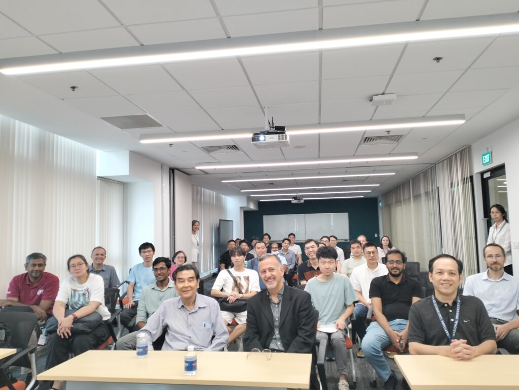
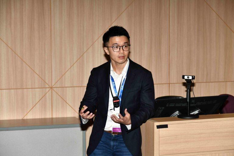
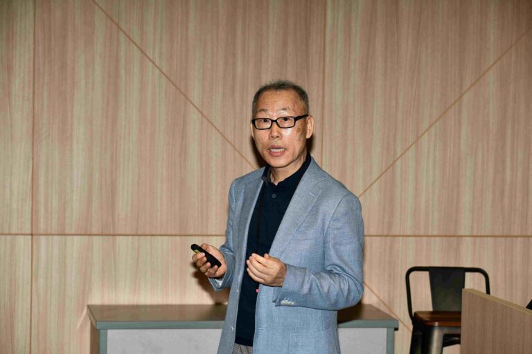
SHINE Management was honoured to host Professor Ali Shakouri from the Birck Nanotechnology Centre, Purdue University (USA), for an insightful seminar on “Nanoscale Thermal Transport and Characterisation for Heterogeneous Integration.” His visit provided an excellent opportunity for our community to engage with leading perspectives on nanoscale thermal behaviour, advanced metrology, and integration-driven research directions for next-generation electronics.
Seminar Highlights
Nanoscale Thermal Transport Physics Professor Shakouri began by outlining the fundamental principles governing heat conduction at the nanoscale, establishing the physics foundation for understanding thermal behaviour in advanced materials and device architectures.
Advanced Characterization and Metrology He then discussed state-of-the-art tools and techniques for thermal measurement, including image-processing-enabled fast thermal simulations and far-field thermoreflectance methods capable of achieving sub-diffraction-limit thermal imaging down to approximately 100 nm through image deconvolution. These approaches highlighted the growing importance of accurate, high-resolution thermal characterization for 3D ICs and heterogeneous systems.
Integration-Oriented Research Directions The seminar further explored multiscale and system-level thermal challenges in heterogeneous integration. Key themes included interface and interconnect thermal resistance, in-plane and through-plane thermal coupling in 2.5D/3D stacks, transient versus steady-state thermal behaviour under operational loads, and emerging data-driven and AI-assisted approaches for predictive thermal analysis.
The seminar concluded with strong participation and a lively Q&A session that encouraged in-depth discussion and critical engagement, reflecting the session’s significant contribution to advancing understanding in nanoscale thermal transport and characterization.
Exclusive NUS Talk: imec CTO Live November 17, 2025
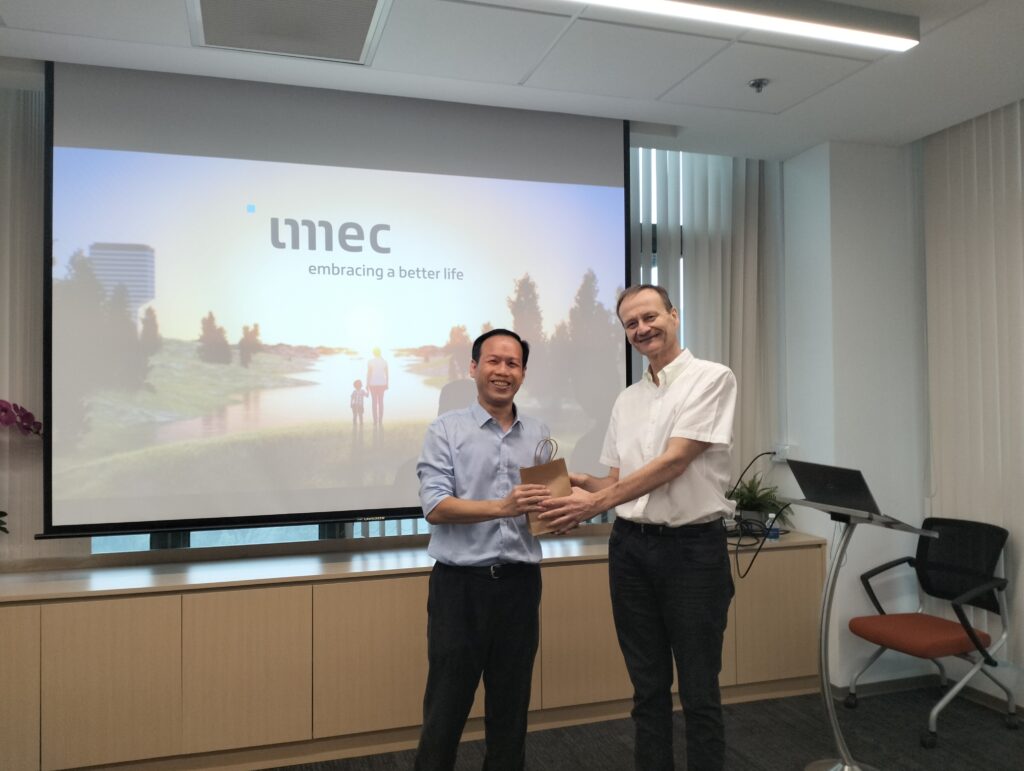
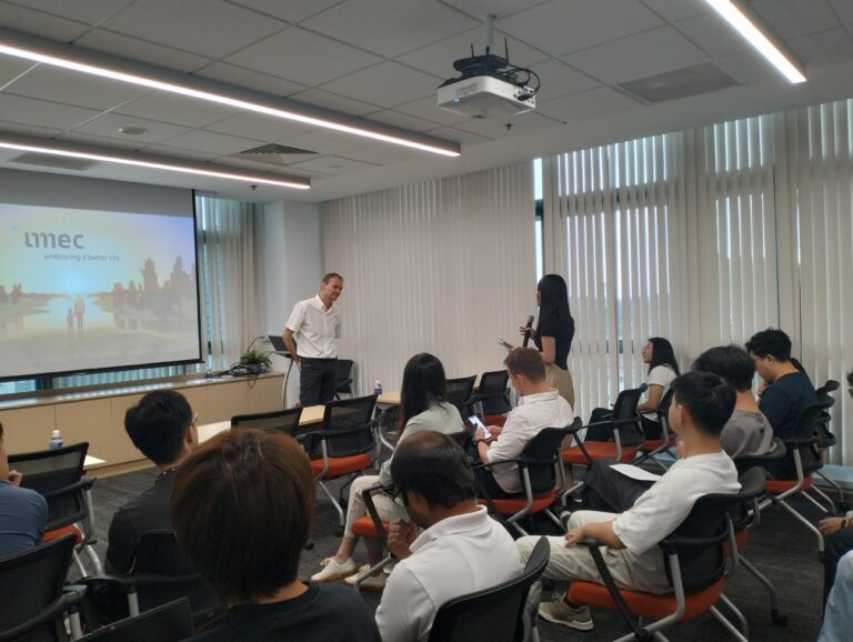
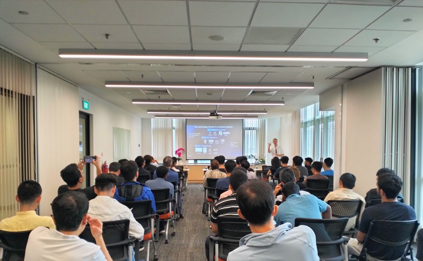
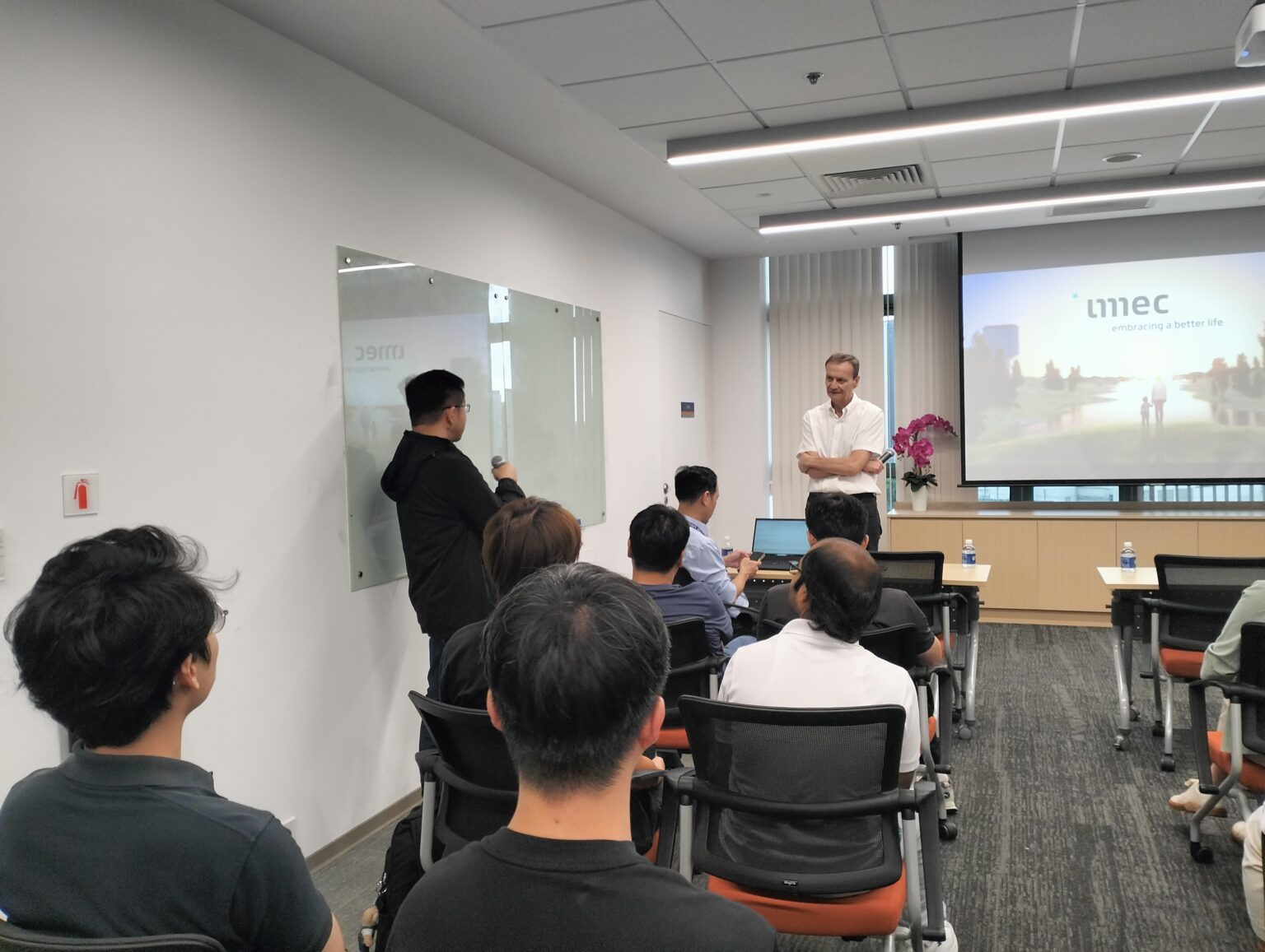
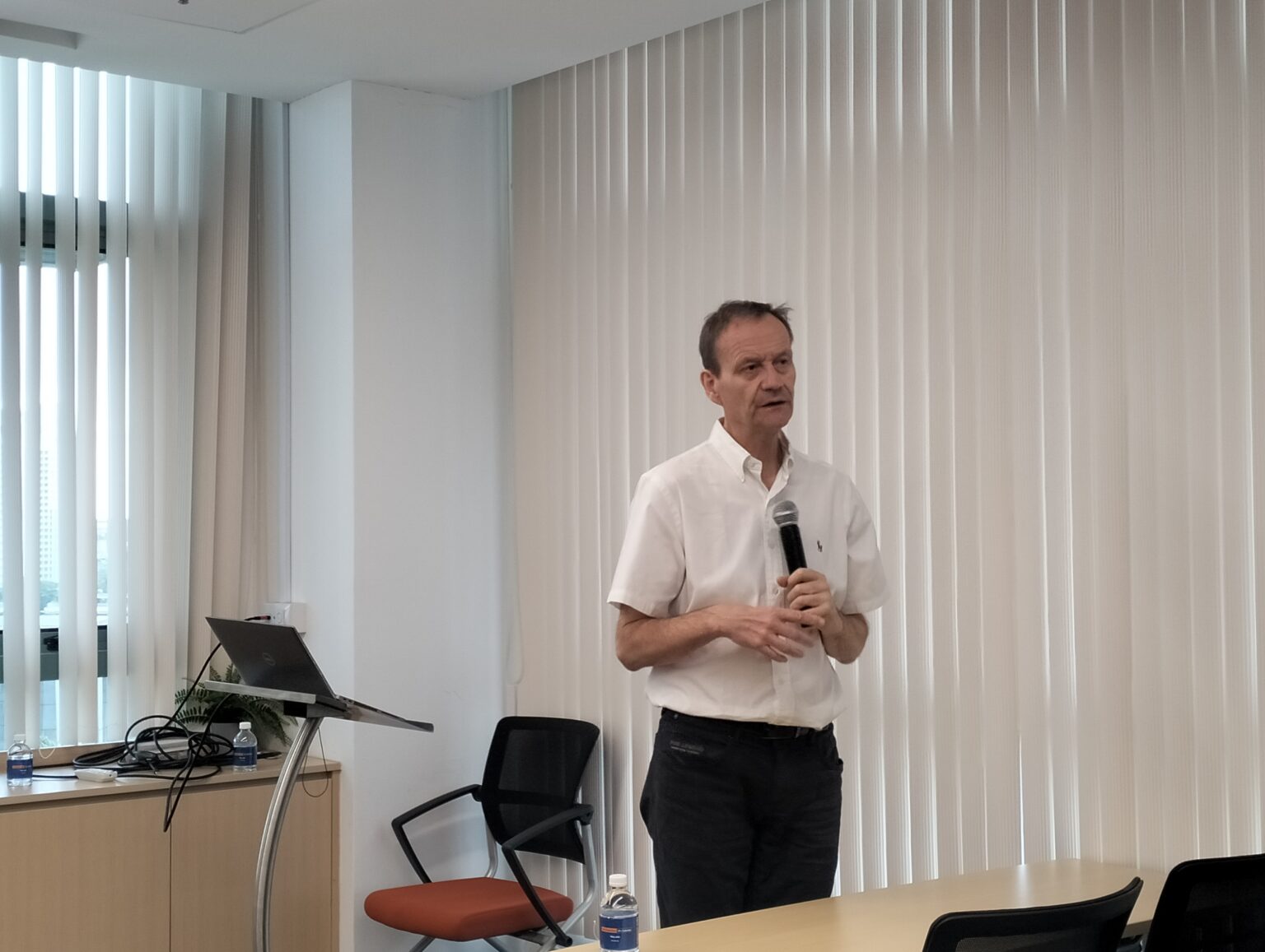
SHINE Management gratefully acknowledges Dr. Paul Heremans for his intellectually enriching and forward-looking contribution to the “Exclusive NUS Talk: imec CTO Live” on 14 November 2025. His insights offered a comprehensive perspective on emerging trends and future directions in semiconductor and photonic technologies.
The session explored the future of these technologies through the lens of imec, the world’s largest independent research and innovation centre for nanoelectronics and digital technology. Founded in 1984, imec is a global leader in nanoelectronics, widely recognized as the “chip lab of the world.” Its research advances smaller, faster, and more energy-efficient chips, addressing pressing global challenges such as climate change, healthcare, and food security. imec’s innovations impact diverse sectors, including consumer electronics, healthcare, and energy systems.
In his seminar, Dr. Paul Heremans articulated imec’s strategic vision and highlighted key research directions including:
Core semiconductor technologies for next-generation process nodes
Silicon photonics for quantum computing and photonic control of neutral atoms, ions, and NV centres
imec’s strong connection with the academic world nurtures innovative excellence
Participants gained a deeper understanding of major technological challenges, emerging trends, and practical implications for both academia and industry. The seminar concluded with a dynamic Q&A session, reflecting attendees’ engagement and curiosity, underscoring the ongoing relevance and impact of imec’s research in shaping the future of technology.
Silicon Programmable Photonic Circuits for AI Computing November 12, 2025
Silicon Programmable Photonic Circuits for AI Computing
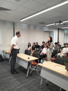
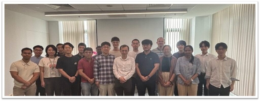
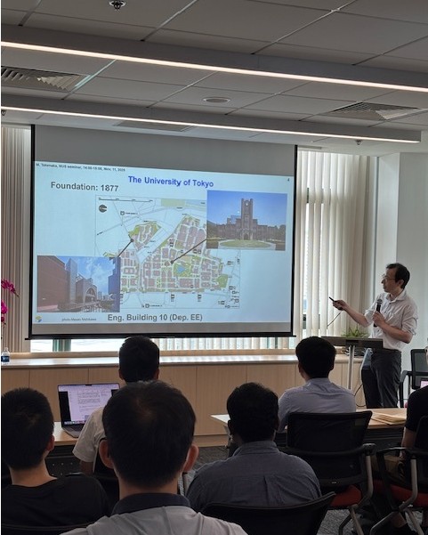
SHINE Management extends its heartfelt appreciation to Prof. Mitsuru Takenaka from The University of Tokyo for delivering an inspiring and thought-provoking seminar on “Silicon Programmable Photonic Circuits for AI Computing.”
During the talk, Prof. Takenaka shared how recent advances in silicon-based programmable photonic circuits—made possible through the integration of heterogeneous materials – are unlocking novel device concepts, circuit architectures, and experimental methods. These developments highlight silicon photonics as a scalable, energy‑efficient platform for next‑generation AI hardware.
Key takeaways included:
Photonic processors that enable low-energy multiply–accumulate (MAC) operations.
Hybrid systems utilizing light for weight distribution and progressing toward fully photonic architectures, with an engaging discussion on achieving the optimal balance between optical and electronic processing.
The critical role of electronic–photonic integration as a foundation for practical quantum systems.
The potential for large-scale integration beyond the 128×128 threshold.
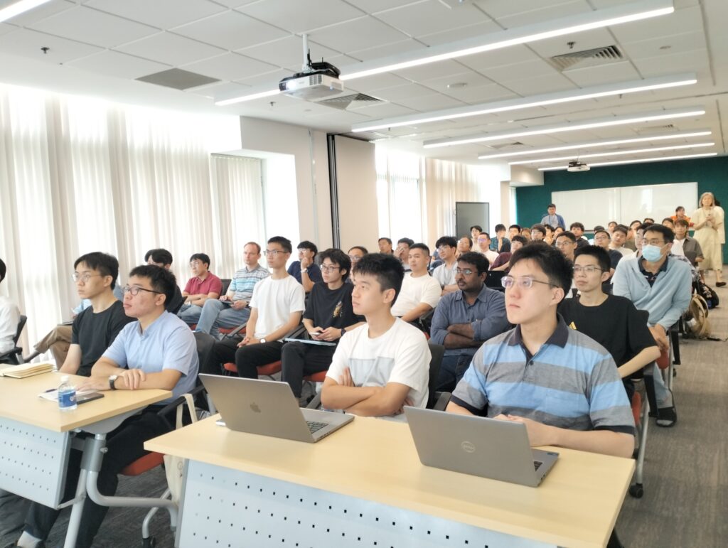
The talk drew an extremely strong turnout and was overwhelmingly well received on the floor, culminating in an energetic, extended questions and answers session. The session closed with clear interest in collaborations and follow-up demonstrations, underscoring the momentum behind silicon photonics for next-generation AI and quantum hardware.
FDSOI platform – Leveraging Semiconductor Industry for Large Scale Quantum Computing October 24, 2025
Leveraging Semiconductor Industry for Large Scale Quantum Computing
SHINE Management is honoured to express its sincere appreciation to Dr. Maud Vinet, Co-Founder and CEO of Quobly, for her distinguished and insightful presentation on the path to scalable quantum computing with silicon.
The talk highlighted why Si-based qubits are a leading candidate for scaling, leveraging mature semiconductor manufacturing and the prospect of co-integrating qubits with transistors to keep large quantum circuits comparable in footprint to classical processors.
Dr. Vinet presented FDSOI CMOS as a practical platform to co-integrate spin qubits with integrated control/read-out circuits, and shared recent advancements in quantum dot arrays, demonstrating elementary operations at microsecond timescales with state-of-the-art noise performance.
The session also covered FDSOI-based cryo-control electronics, demonstrating elementary control and read-out at cryogenic temperatures, and outlined strategies, as well as key challenges, for co-integrating qubits and integrated circuits at advanced technological nodes.
Participants left with a clearer view of how industry-compatible technologies can accelerate the engineering of “good qubits” and the roadmap to large-scale silicon quantum processors.
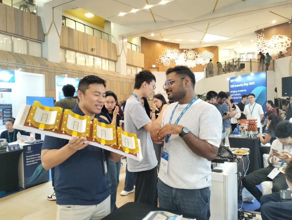
SHINE at CDE Industry Day 2025 September 26, 2025
SHINE CENTRE Showcases at CDE Industry Day 2025
Date : 26 September 2025
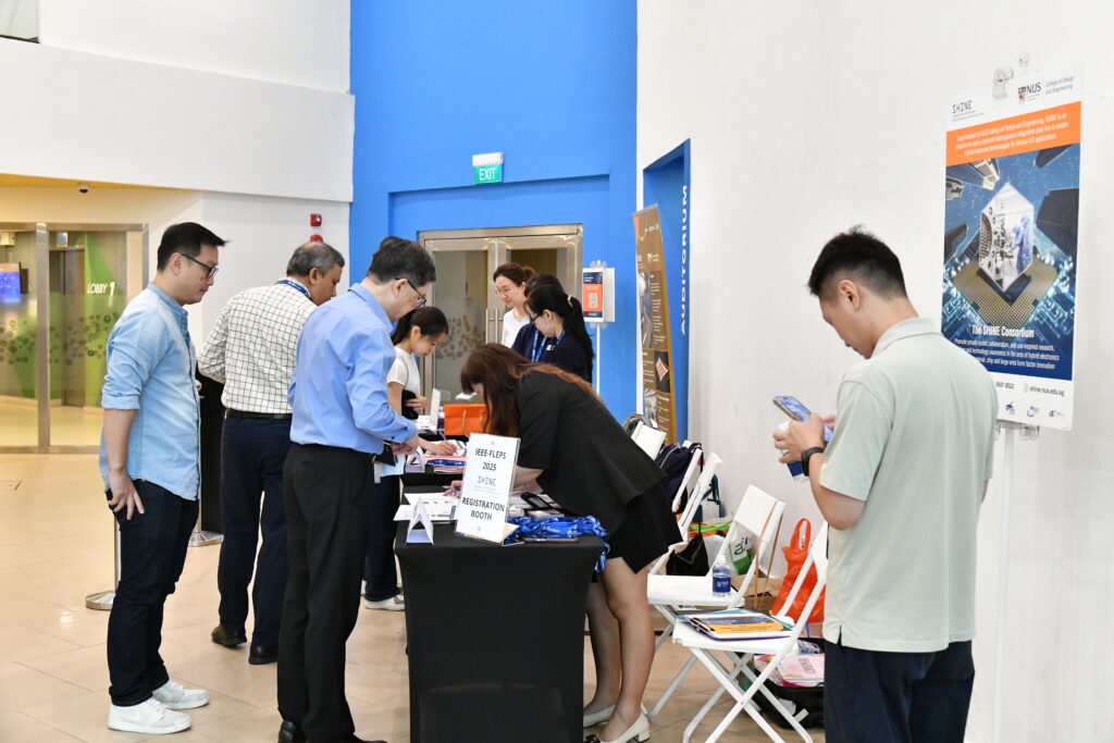
On 26 September 2025, SHINE NUS participated in the College of Design and Engineering (CDE) Industry Day 2025, held at the National University of Singapore (NUS). The biennial event brought together industry leaders, researchers, and students to explore opportunities for collaboration, knowledge exchange, and innovation.
At the exhibition, SHINE presented its latest initiatives, and partner projects with a focus on: 1) Fully flexible, light weight and conformal antenna array using polyimide films, mesh patterns (corrugated and uneven etc.,) 2) Enabling interactive and intuitive understanding of complex 3D-IC structures 3) The development of advanced hybrid interposer structures for high power system packaging and heterogeneous integration 4) HZO-LNOI integrated ferroelectric electro-optic modulator and memory 5) High-speed die temperature control for GPU wafer-level testing 6) Heterogeneous integration on low-dimensional (near-1D) and e-textile ultra-low power systems
The booth attracted strong interest from faculty members, industry partners, and visitors, serving as a valuable platform to exchange insights and explore potential collaborations.
The event also featured networking sessions and a walk-through by CDE leadership along with VIPs, during which SHINE’s contributions were highlighted as part of NUS’s ongoing efforts to foster impactful partnerships between academia and industry.
As part of the programme, SHINE hosted a lab tour, providing guests with an in-depth look into the forefront of semiconductor and electronics research.
Participation in CDE Industry Day 2025 provided SHINE with an important opportunity to showcase its work, strengthen connections with partners, and explore avenues for future collaboration. SHINE remains committed to driving innovation that addresses real-world challenges through strong partnerships with both academia and industry.
AI for Chip Design: Hype or Reality? September 15, 2025
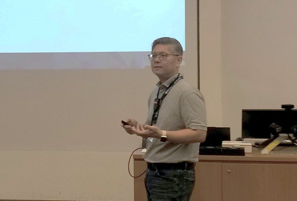
SHINE management was honoured to welcome Prof. Alberto Sangiovanni-Vincentelli, Edgar L. and Harold H. Buttner Chair at the University of California, Berkeley, for a seminar held at NUS on 15 September 2025. He delivered a thought-provoking talk titled “AI for Chip Design: Hype or Reality?”, which sparked engaging discussions among faculty, researchers, and students.
In his talk, Prof. Sangiovanni-Vincentelli critically examined the transformative promise of Artificial Intelligence (AI) in chip design and development. He explored the rapid rise of AI, driven by the explosion of big data and advances in computing power, and unpacked the evolution of key technologies including Machine Learning, Deep Learning, and Generative AI.
The seminar provided a nuanced look at AI’s real-world impact and highlighting both its potential and limitations. Prof. Sangiovanni-Vincentelli also shared practical case studies from the chip industry, offering insights into how these technologies are being applied today.
We thank Prof. Sangiovanni-Vincentelli for an engaging and thought-provoking session that sparked meaningful discussions within our research community.
SHINE 6th Technical Workshop June 30, 2025
SHINE 6th Technical Workshop
Date : 24 to 25 June 2025 | Venue: Block EA, 9 Engineering Drive 1, NUS College of Deisgn and Engineering
The SHINE Open Plenary, held as part of the SHINE 6th Technical Workshop at NUS, followed the SHINE-sponsored IEEE FLEPS 2025 Industry Plenary in the morning. The Open Plenary session, from 2:00 pm to 3:35 pm, was open to the public and provided a platform for knowledge exchange on cutting-edge developments in hybrid electronics and advanced materials.
The session commenced with a welcome address by Prof. Chen Xiaodong, Deputy Director of SHINE Centre, who reiterated SHINE’s commitment to breakthroughs in material innovation, flexible electronics, and heterogeneous integration. Prof. Chen emphasized the vital role of collaborative partnerships in advancing the field and translating research into impactful solutions.
Three distinguished industry speakers were featured during the SHINE open plenary sssion:
Prof. Ng Geok Ing (Centre Director, National GaN Technology Centre, NTU) presented recent advances and market projections for GaN-on-Si technology in RF applications, especially for 5G/6G and low-voltage mobile mmWave front-ends. He showcased NGTC’s infrastructure and capabilities in rapid prototyping and small-volume production, underscoring both the challenges and opportunities in commercializing RF GaN-on-Si technology, as well as the importance of developing a robust local ecosystem.
Dr. Luo Xianshu (Vice President of Advanced Photonics, NSTIC) discussed the evolution of silicon photonics and its critical role in enabling high-speed, low-cost optical transceivers for data centers. He outlined the limitations of traditional silicon photonics, the need for heterogeneous material integration, and NSTIC’s progress in new material platforms such as H-free CVD SiN and AlN-based photonics to drive next-generation device performance and manufacturability.
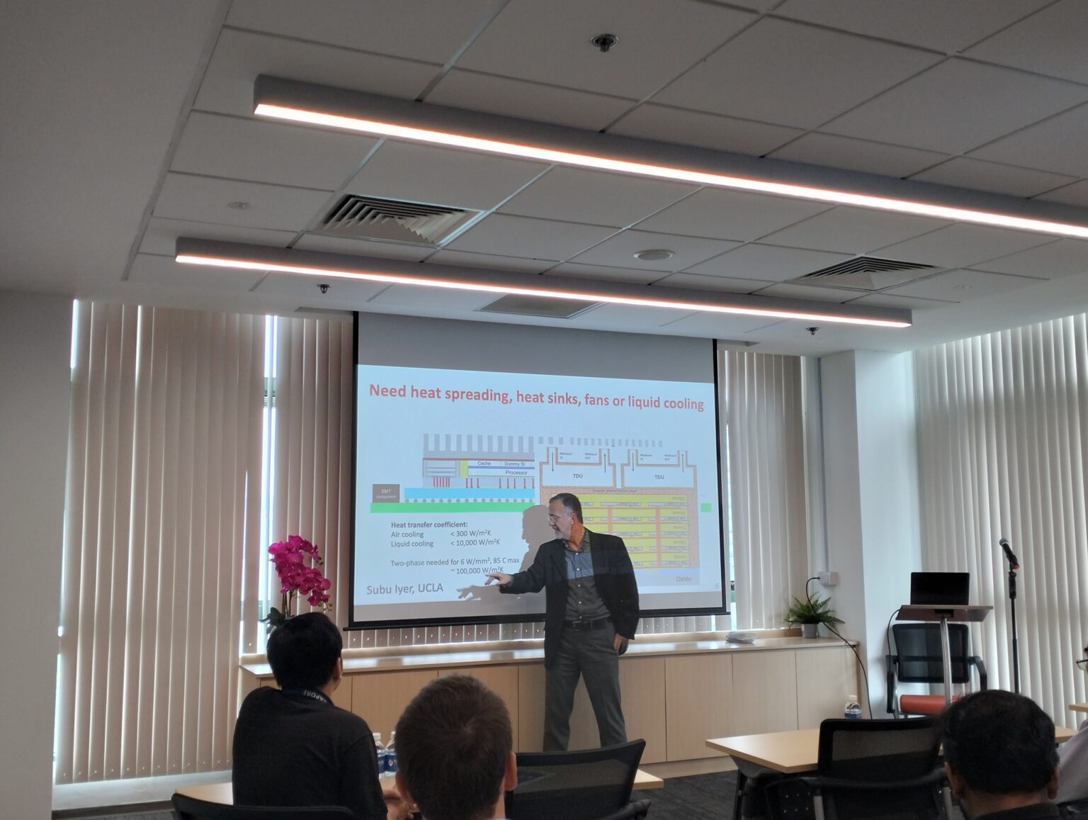
Mr. Vempati Srinivasa Rao (Director, Heterogeneous Integration, A*STAR IME) highlighted advanced packaging technologies enabling multi-chiplet heterogeneous system-in-package (SiP) solutions for generative AI and high-performance computing (HPC). He detailed IME’s initiatives in interconnect scaling, packaging for AI/HPC, system-level thermal management, and collaborative R&D efforts with industry and academia to accelerate innovation in advanced packaging.
Technical Presentations and Consortium Sharing (Closed Sessions):
Following the Open Plenary, the technical workshop sessions were accessible exclusively to SHINE consortium members and the research community. Over the two-day workshop from 24 to 25 June 2025, eight presentations covered SHINE’s four project thrusts, including:
Novel Ultra-low Power Chiplet Architectures – Featuring SHINE chiplet systems across the entire system lifecycle and silicon case studies by Prof Massimo Alioto of NUS, SHINE Thrust 1 Co-Investigator.
Advanced Materials Chemistry – Featuring conformal bioelectronics for human-machine interfaces by Prof Chen Xiaodong of NTU, SHINE Thrust 2 Co-Investigator.
3D Printable Ink Solutions for Thermal Management and Energy Harvesting – Focusing on soft electronics by Dr Hyunwoo Bark of NTU, SHINE Thrust 2 Senior Research Fellow.
Two-tiered Failure Analysis Approach – Combining Electromagnetic Frequency Domain Analysis (EM-FDA) and Magnetic Field Imaging (MFI) by Dr Lucus Lum of NUS, SHINE Thrust 4 Research Fellow.
Non-Hermitian Thermophotonic Funnelling – Offering new insights for nanoscale energy and information manipulation by Mr Yang Shui Hua of NUS, SHINE Thrust 4 PhD Student.
Integration towards Phased Arrays – Addressing beam distortion caused by deformation in phased array antennas by Dr Jiang Yi Zhou of NUS, SHINE Thrust 3A Research Fellow.
Miniaturized Transceivers – Covering circuit analysis, packaging concepts, and the performance of RF-HI chips for multi-band data communication by Mr Soh Chee Hong
Flexible and Conformal Phased Arrays – For communication and remote sensing systems by Dr Mohammed Ameen of NUS, Thrust 3B Research Fellow.
The SHINE 6th Technical Workshop provided attendees with valuable insights into emerging technologies, industry trends, and collaborative opportunities across hybrid electronics and related fields. The event reinforced SHINE’s pivotal role in fostering a hybrid-integrated next-generation microelectronics system ecosystem and expediting the translation of academic research into practical, industry-ready innovations.
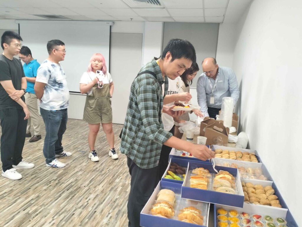
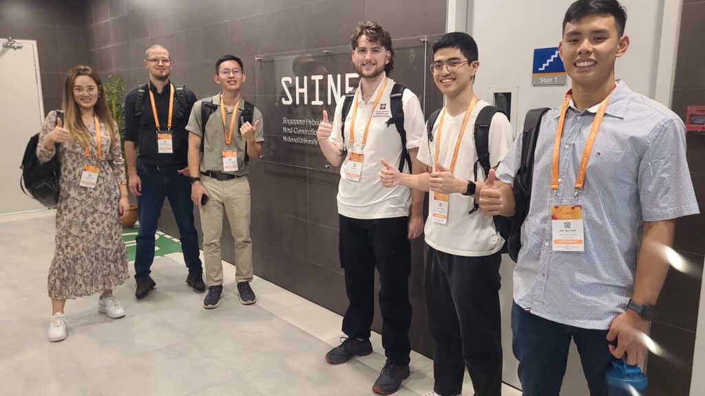
The Photo Gallery
SHINE-led IEEE FLEPS 2025 Industry Plenary June 29, 2025
Post Event Report
SHINE-led IEEE FLEPS 2025 industry Plenary
SHINE-led IEEE FLEPS 2025 Industry Plenary
In conjuction with SHINE 6th Technical Workshop
Time: 8.30 am to 2.00 pm | Venue: Block EA, LT7A, College of Design and Engineering
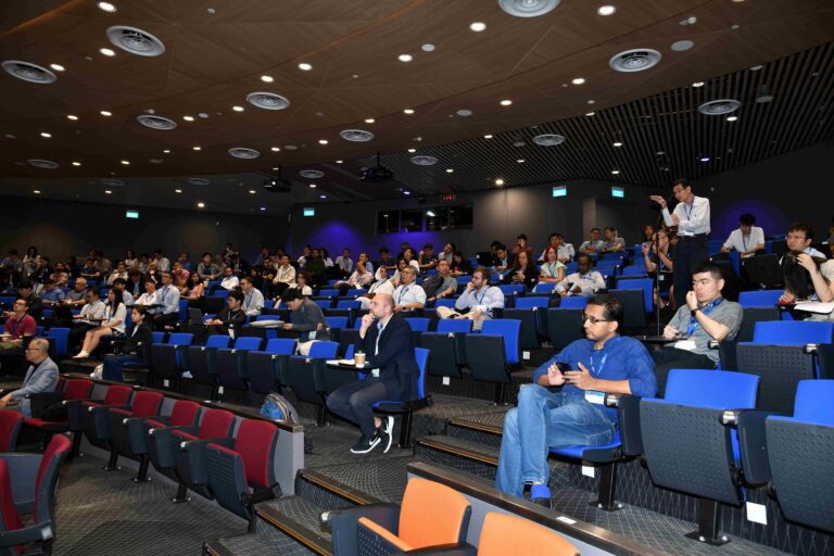
For the first time, SHINE was pleased to host the IEEE FLEPS2025 Industry Plenary as part of its Bi-annual 6th Technical Workshop, bringing together leading experts and innovators at the NUS College of Design and Engineering. This landmark collaboration highlighted the latest advancements shaping the future of semiconductor packaging, flexible hybrid electronics, and automotive interface design. Throughout the morning session, distinguished industry leaders shared transformative breakthroughs in smart manufacturing, innovative material solutions, and simulation-driven design, underscoring the critical need for intelligent, adaptable, and cost-effective solutions to enable next-generation technologies. The plenary attracted a diverse and enthusiastic audience from both academia and industry, setting the stage for vibrant idea exchange and collaboration.
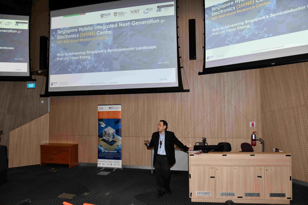
The session opened with Prof. Lim Yeow Kheng, who spotlighted SHINE’s leadership in heterogeneous integration and hybrid microelectronics, including initiatives such as the SHINE Lighthouse Project and a local “Mix-&-Match” pilot line enabling rapid translation of research breakthroughs into industrial applications and strengthening Singapore’s position in the global microelectronics landscape. By fostering cross-disciplinary research and collaboration among academia, research institutes, and industry, SHINE serves as a national platform to develop next-generation flexible and hybrid electronic systems.
Several distinguished industry plenary speakers during the event included:
Chris Sim, Director of Package Development Engineering at Micron Technology, shared smart manufacturing AI and digital twin technologies are transforming semiconductor packaging. He highlighted advancements in system-level co-design, predictive models, and process controls that enhance efficiency, quality (predictive outputs), and agility well- aligned with Industry 4.0. Mr. Sim also outlined Micron’s strategic innovations across HBM, NAND, and DRAM, showcasing the role of intelligent manufacturing in driving next-generation semiconductor solutions.
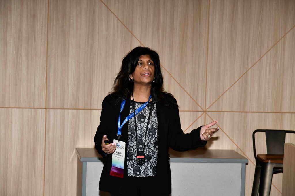
Madhu Stemmermann, CEO of SunRay Scientific, introduced ZTACH® Anisotropic Conductive Epoxy (ACE), a magnetically aligned conductive epoxy that enables superior adhesion, reliable, cost-effective interconnections for Flexible Hybrid Electronics (FHE) using existing SMT lines. She highlighted its ease of integration, low-temperature processing, and versatility across applications, including smart labels, RFID tags and wearables, exemplifying its potential to simplify FHE manufacturing and accelerate adoption across industries.
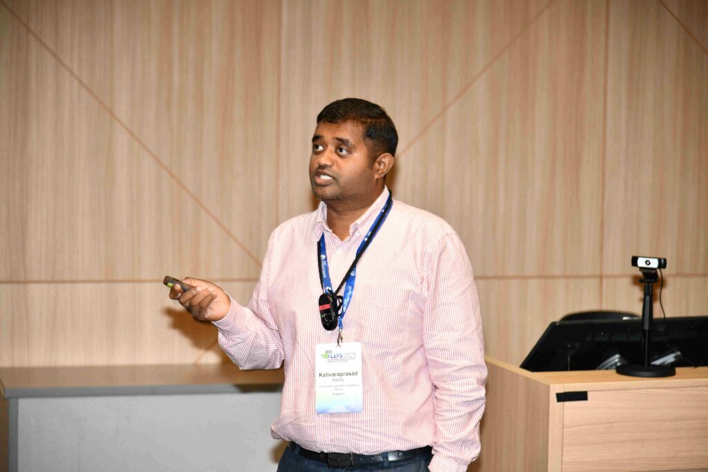
Mr Dontireddy, Kalivaraprasad Reddy from Continental Automotive shared insights on the design and challenges of automotive display interfaces. He discussed the use of flexible printed circuit boards (PCBs) for modern vehicle interiors, highlighting their advantages in fitting compact spaces while also addressing critical signal integrity concerns that posed electromagnetic compatibility (EMC) issues. Advanced simulations enable early detection and resolution of these challenges, ensuring high-quality, cost-effective designs that support the future of connected, sustainable, and intelligent mobility solutions.
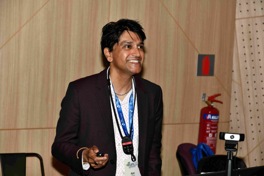
Dr. Ajay Virkar, Vice President of Advanced Circuits and Packaging at DuPont (USA), introduced DuPont’s ActivegridTM, a flexible, stretchable silver nanowire-based transparent conductor that outperforms conventional materials. Compatible with low-temperature, high-speed processing, ActivegridTM is integrated into flexible consumer electronics and is expanding into emerging applications, including smart windows, transparent EMI shielding, photovoltaics, displays, biomedical devices, and automotive sensor heating. He also highlighted recent advances in concentrated silver nanowire inks and materials as advanced fillers, enabling next-generation flexible and printed electronics.
Dr. James Lee, Deputy Chief Engineer at TCL Corporate Research, discussed TCL’s flexible printed OLED TV technology, enabling rollable, scrolling and foldable “TV Mobiles” integrated with sensors, AI, and 5G/6G connectivity. Key breakthroughs include advanced oxide TFTs, top-emission OLEDs, MURA-free printing, advanced thin film encapsulation, and cost- efficient mechanical release technology. TCL’s 31” 4K flexible OLED TV demonstrates high resolution, excellent contrast, wide colour gamut, and tight curvature, marking crucial progress in performance and production.
Dr. Sudheer Kumar, Chief Operating Officer at the National Centre for Flexible Electronics, Indian Institute of Technology Kanpur, presented advancements in Flexible Hybrid Electronics (FHE), which integrates printed electronics with traditional semiconductors to enable lightweight, bendable systems. He emphasized the need for direct-write technologies, reduced metal content, and low-temperature processing to meet evolving market demands. The talk also highlighted material property control as the key to device performance, with emerging applications in advanced packaging and healthcare.
Mr. Shimizu Ryota, Chief of R&D at Satosen Corporation, Japan, presented a stretchable PCB technology using liquid metal channels embedded in elastomers, offering enhanced flexibility, durability, and reliable conductivity. He highlighted its scalable fabrication process and potential for wearable electronics and flexible sensors, demonstrating strong electrical performance and mechanical robustness under strain, advancing the development of highly deformable electronic devices.
This inaugural SHINE-hosted IEEE FLEPS2025 Industry Plenary not only demonstrated the industry’s rapid progress but also paved the way for deeper collaborative innovation in flexible electronics, printable sensors and semiconductor technologies.
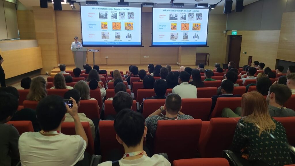
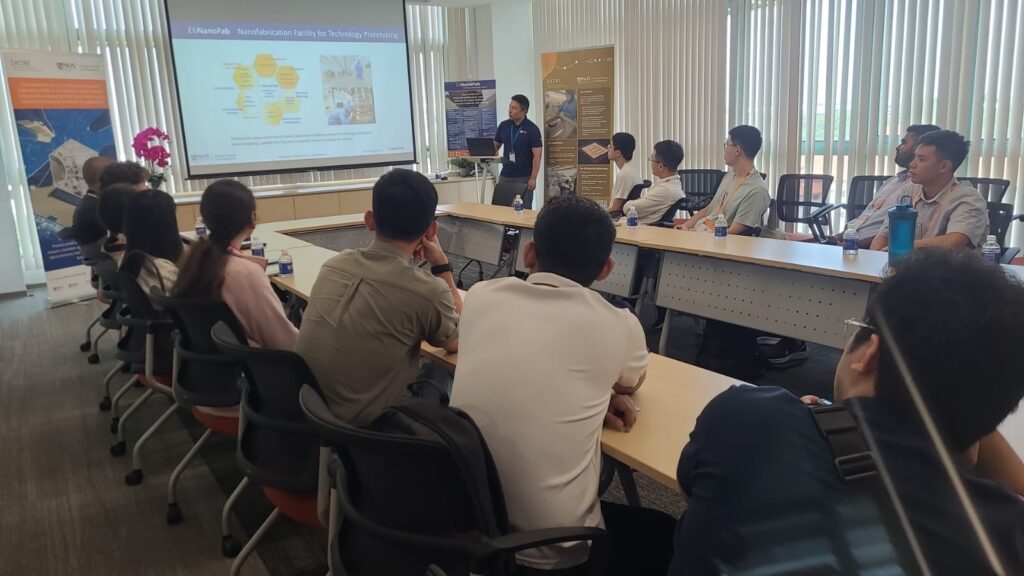
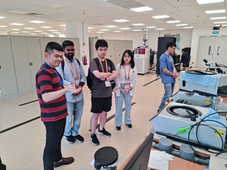
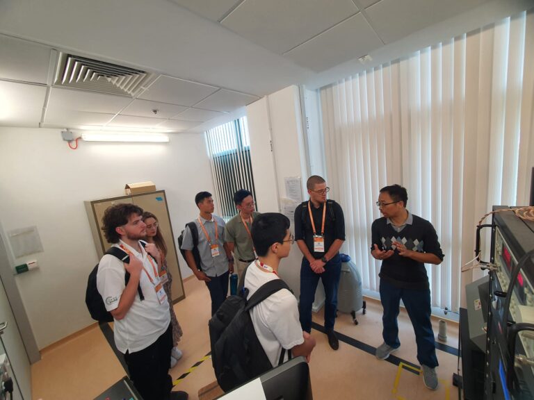
On the last day of IEEE FLEPS2025, SHINE hosted 25 attendees for an exclusive tour of the SHINE Advanced Packaging Centre and the E6NanoFab—NUS’s state-of-the-art nano-microelectronics research facilities. Led by David Xu, E6NanoFab’s process engineering RF lead, participants received an overview of the facilities before visiting advanced stations for lithography, etching, deposition, metrology, characterisation, and packaging.
This behind-the-scenes experience offered guests firsthand insights into Singapore’s world-class innovation infrastructure, highlighting the strong synergy between cutting-edge research and industrial application. The tour served as an inspiring finale to the conference, reinforcing SHINE’s pivotal role in driving collaboration and advancing the future of flexible and hybrid electronics.
The Photo Gallery
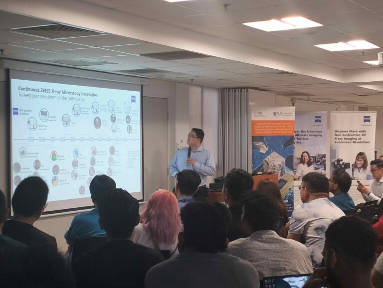
SHINE ZEISS Joint Seminar: Exploring Defects & Structures. Microscopy Solutions for Advanced Semiconductor Packaging March 13, 2025
SHINE ZEISS Joint Seminar | 13 March 2025
Exploring Defects and Structures. Microscopy Solutions for Advanced Semiconductor Packaging
On 13th March, the NUS SHINE & ZEISS Joint Seminar on Non-Destructive 3D Imaging and AI-Driven Deep Learning for Semiconductor Materials drew close to 55 attendees, providing a deep dive into the latest advancements in semiconductor failure analysis.
The event commenced with an opening address by Prof. Lim Yeow Kheng, Programme Director of SHINE who emphasized that failure analysis is a crucial aspect of the semiconductor industry and that researchers must think ahead of their time. He highlighted the growing importance of AI-enhanced imaging in semiconductor research, which accelerates failure analysis. He encouraged attendees to make the most of the sharing session by learning and exchanging information.
The seminar featured expert speakers from academia and industry, offering insights into how X-ray Computed Tomography (CT), machine learning (ML), and correlative microscopy are transforming defect detection, predictive diagnostics, and material characterization.
The seminar’s technical discussions covered a range of innovative methodologies:
Dr. Sky Xie, ZEISS Research Microscopy Solutions Sales Specialist, introduced deep-learning-enhanced X-ray CT, showcasing its ability to improve imaging efficiency while preserving defect details.
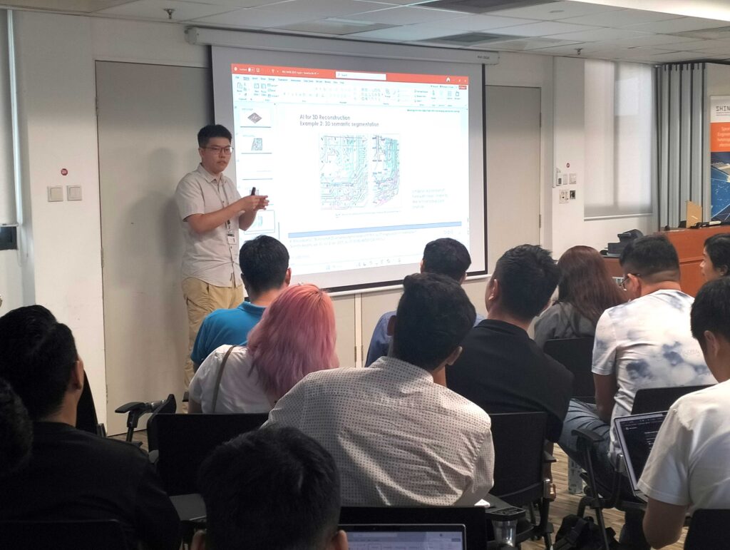
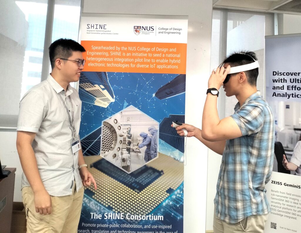
Mr. Shi Zhansen, Research Engineer at NUS SHINE Centre, explored the integration of X-ray imaging with machine learning to advance electronic digital twins, enabling precise defect localization and circuit reconstruction. His talk also featured a VR demonstration, offering an immersive perspective on circuit analysis and reconstruction.
Dr. Riko I Made, Scientist at A*STAR, discussed the role of ML in X-ray CT for automated defect detection and predictive failure modeling.
Dr. Feng Lin Ng, APAC Materials Research and Research Microscopy Solutions Business Development Specialist at ZEISS, demonstrated a correlative microscopy workflow that bridges multi-scale imaging techniques for targeted semiconductor research.
The seminar provided a platform for meaningful discussions and cross-disciplinary collaborations, with participants engaging in thought-provoking exchanges on the future of AI-driven imaging in semiconductor diagnostics. The event concluded with an interactive quiz, reinforcing key takeaways from the presentations.
NRF’s Global Young Scientist Summit (GYSS) Visit to SHINE Centre January 6, 2025
NRF’s Global Young Scientist Summit (GYSS) Visit to SHINE Centre
Date: 16 Jan 2025
Venule: Block E6, 5 Engineering Drive 1 S(117608)
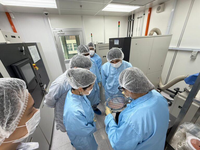
On 6 January 2025, the SHINE Centre, hosted by the NUS E6NanoFab, welcomed the PhD students and young doctorate researchers participating in the esteemed National Research Foundation (NRF)’s 2025 Global Young Scientist Summit (GYSS). The annual NRF’s GYSS event convenes young scientists from around the world to address critical global challenges through scientific research and innovation.
The tour serves to provide a glimpse into the forefront of semiconductor manufacturing technology and facilities of SHINE Centre and E6NanoFab, situated within the NUS College of Design and Engineering campus.
Meanwhile, we’d like to thank the facilities’ research fellows, engineers and technical staff for the comprehensive tour path ensuring attendees were exposed to cutting-edge technologies in deposition, lithography, metrology, characterization, and packaging. Also, a special shout out to the Enrico and Xiao Ya of POET Technologies, SHINE’s industry collaborator for the live demonstration of SHINE’s state of the art Precision Bonding and Assembly in Flip Chip Technology, Pick &-Place Integration Scaling, Advanced Material Processing, and Co-Packaged Optics Capability.


")
")
")


")


 cropped")