Sidebar


Publications – 2022   SHINE


A 1.3-Micrometre-Thick Elastic Conductor for Seamless On-skin and Implantable Sensors

Publication

On-skin and implantable electronics require elastic conductors that are only a few micrometres thick and soft enough to form a seamless contact with three-dimensional structures. However, fabricating thin conductors that are mechanically durable and have consistent electrical properties with stretching is challenging. Here we report polydimethylsiloxane (PDMS)–gold conductors that are around 1.3 µm thick and have a controlled morphology of microcracks in the gold film. 

The microcracks are formed by evaporating a 50-nm-thick gold film onto a 1.2-µm-thick PDMS film that is supported during fabrication by a 100-µm-thick PDMS film on glass; thermal expansion of the thick PDMS film causes the evaporated gold to form a microcracked structure on the thin PDMS. The resulting conductors can be stretched by up to 300% and remain highly conductive after strain release. We use them to create on-skin electrodes that are breathable and water resistant, and can continuously record electrocardiogram signals. We also use the conductors to create on-skin sensors with less than 3 µm thickness that can detect small mechanical forces and create implantable nerve electrodes that can provide signal recording and stimulation.

Researcher/Author: (1) NTU – Zhi Jiang, Nuan Chen,  Feilong Zhang, Shaobo Ji,  Xiaodong Chen (2) NUS – Zhigao Yi,Ji Shaobo, Xiaogang Liu (3) UM – Junwen Zhong (4) UESTC – Rui Liao, Yang Wang (5) UOT – Yan Wang, Tomoyuki Yokota, Takao Someya  (6) A*STAR IME – Haicheng Li, Zhihua Liu (7) CEMS – Kenjiro Fukuda.


Nat Electron 5, 784–793 (2022)
https://www.nature.com/articles/s41928-022-00868-x

Robust Beamforming for Space-based SAR Phased Arrays with Distributed Interferer Suppression

Publication

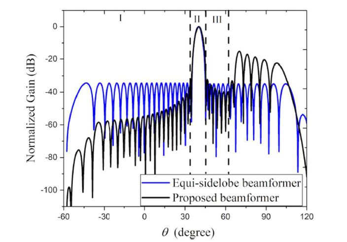
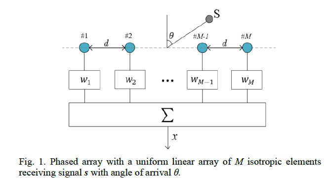
Synthetic aperture radar (SAR) is one of the remote sensing technologies used for Earth observation missions. Phased arrays combined with adaptive beamforming can be used in SAR to improve system performance [1]. In commonly used adaptive beamformers, such as the minimum variance distortionless response (MVDR) beamformer, the angles of
arrival from desired signals and interferers are provided with discrete values and the beamforming weights are computed to
keep desired signals and to suppress interferers at the respective angles [2]. However, interferers may not be located
at known discrete angles and may, instead, be distributed over a range of angles. Then traditional beamformers work less
well as some interferers are suppressed while others are not. Here, a beamforming technique is presented that incorporates
the probability density of the distribution of interfering signals.

Researcher/Author: Jiahao Wang (NUS), Koen Mouthaan (NUS).

2022 International Symposium on Antennas and Propagation (ISAP) 31 Oct – 3 Nov.  https://ieeexplore.ieee.org/document/9998656


Reconfigurable nonlinear photonic activation function for photonic neural network based on non-volatile opto-resistive RAM switch

Publication

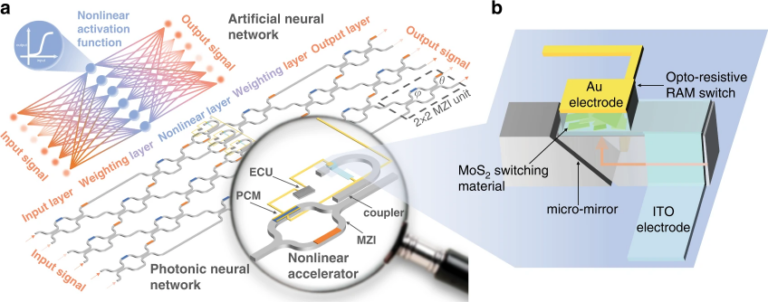
Photonic neural network has been sought as an alternative solution to surpass the efficiency and speed bottlenecks of electronic neural network. Despite that the integrated Mach–Zehnder Interferometer (MZI) mesh can perform vector-matrix multiplication in photonic neural network, a programmable in-situ nonlinear activation function has not been proposed to date, suppressing further advancement of photonic neural network. Here, we demonstrate an efficient in-situ nonlinear accelerator comprising a unique solution-processed two-dimensional (2D) MoS2 Opto-Resistive RAM Switch (ORS), which exhibits tunable nonlinear resistance switching that allow us to introduce nonlinearity to the photonic neuron which overcomes the linear voltage-power relationship of typical photonic components. Our reconfigurable scheme enables implementation of a wide variety of nonlinear responses. Furthermore, we confirm its feasibility and capability for MNIST handwritten digit recognition, achieving a high accuracy of 91.6%. Our accelerator constitutes a major step towards the realization of in-situ photonic neural network and pave the way for the integration of photonic integrated circuits (PIC).

Researcher/Author: Zefeng Xu (NUS), Baoshan Tang (NUS), Xiangyu Zhang, (NUS) Jin Feng Leong (NUS), Jieming Pan (NUS), Sonu Hooda (NUS), Evgeny Zamburg (NUS), Aaron Voon-Yew Thean (NUS)

Light Sci Appl 11, 288 (2022)

Passively Aligned Flip-chip Laser Diodes using Multi-axial Slide-stop Guided Design and Laser Assisted Bonding (LAB) on a CMOS-based Optical Interposer

Publication

Silicon photonics (SiPh) has been considered the mainstay for the development of 800G and beyond optical communication technology [1]. As such, SiPh has seen increasing demand for applications in on-chip signaling and data processing. This is in part, due to its low latency, CMOS-compatibility, near-zero electromagnetic interference and the potential for large bandwidth.

In this work, we showcase using a multi-axial slide-stop guided design and LAB to accomplish flip-chip bonding of P-down passively aligned directly modulated laser (DML) diode array onto the world’s smallest transmit and receive CMOS-based optical interposerTM.

The incorporation of rectangular slide-stop structures improve post-bond accuracy by 1.6X achieving a best-in-class relative axial offset of 0.13μm. High-precision bonder with laser-assisted bonding capability enables heterogeneous integration of optical components with higher packing density due to a small heat-affected zone radius of 280μm.

Researcher/Author: (1) POET Technologies – Simon Chun Kiat Goh; Bo Zhao; James Yong Meng Lee; Suresh Suresh Venkatesan (2) NUS ECE Dept / SHINE – Baochang Xu; Yu Zhang; Siah; Yeow Kheng Lim; Aaron Voon Yew Thean and (3) ASM Amicra – Rappl Sebastian

IEEE Xplore 2022 European Conference on Optical Communication (ECOC) 18 – 22 Sep 2022 Publication Download: https://ieeexplore.ieee.org/xpl/conhome/9979160/proceeding

Freestanding and Scalable Force-softness Bimodal Sensor Arrays for Haptically Body Feature Identification

Publication

Freestanding and Scalable Force-Softness Bimodal Sensor Arrays for Haptic Body-Feature Identification

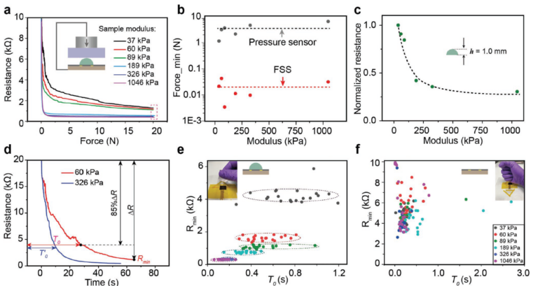
Tactile technologies that can identify human body features are valuable in clinical diagnosis and human–machine interactions. Previously, cutting-edge tactile platforms have been able to identify structured non-living objects; however, identification of human body features remains challenging mainly because of the irregular contour and heterogeneous spatial distribution of softness. Here, freestanding and scalable tactile platforms of force-softness bimodal sensor arrays are developed, enabling tactile gloves to identify body features using machine-learning methods. The bimodal sensors are engineered by adding a protrusion on a piezoresistive pressure sensor, endowing the resistance signals with combined information of pressure and the softness of samples. The simple design enables 112 bimodal sensors to be integrated into a thin, conformal, and stretchable tactile glove, allowing the tactile information to be digitalized while hand skills are performed on the human body. The tactile glove shows high accuracy (98%) in identifying four body features of a real person, and four organ models (healthy and pathological) inside an abdominal simulator, demonstrating identification of body features of the bimodal tactile platforms and showing their potential use in future healthcare and robotics.

Researcher/Author: Zequn Cui (NTU),Wensong Wang (NTU),Huarong Xia (NTU),Changxian Wang (NTU),Jiaqi Tu (NTU) ,Shaobo Ji (NTU),Joel Ming Rui Tan (A*STAR IMRE),Zhihua Liu (A*STAR IMRE),Feilong Zhang (NTU),Wenlong Li (A*STAR IMRE) ,Zhisheng Lv (A*STAR IMRE),Zheng Li (NTU),Wei Guo (NTU),Nien Yue Koh (NTU),Kian Bee Ng (NTU),Xue Feng (Tsing Hua University) ,Yuanjin Zheng (NTU) ,Xiaodong Chen (NTU, A*STAR IMRE)

Advanced Materials, vol. 34, no. 47, 2022,

Impact of Cross Terms on Pattern Multiplication in Receiving Phased Arrays

Publication

Impact of Cross Terms on Pattern Multiplication in Receiving Phased Arrays
The performance of a receiving antenna array can be substantially improved by multiplying the outputs of two colocated receiving arrays. Compared to the performance of the two individual arrays, such multiplication can increase directivity, increase the number of nulls, and reduce sidelobe levels. However, in the multiplication process undesirable cross terms appear which may reduce the potential performance gains. Here, the detrimental impact of correlation between a desired signal and an interfering signal on the cross terms is investigated, as well as the impact of the signal-to-interference ratio on the cross terms. Researcher/Author: Jiahao Wang (NUS), Koen Mouthaan (NUS) 2022 IEEE International Symposium on Antennas and Propagation and USNC-URSI Radio Science Meeting (AP-S/URSI), 2022, pp. 820-821

Physical Insights into Vacancy-Based Memtransistors: Toward Power Efficiency, Reliable Operation, and Scalability

Publication

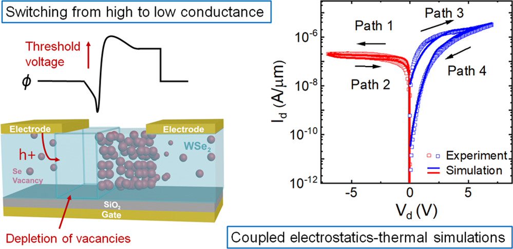
Memtransistors that combine the properties of transistor and memristor hold significant promise for in-memory computing. While superior data storage capability is achieved in memtransistors through gate voltage-induced conductance modulation, the lateral device configuration would not only result in high write bias, which compromises the power efficiency, but also suffers from unsuccessful memory reset that leads to reliability concerns. To circumvent such performance limitations, an advanced physics-based model is required to uncover the dynamic resistive switching behavior and deduce the key driving parameters for the switching process. This work demonstrates a self-consistent physics-based model which incorporates the often-overlooked effects of lattice temperature, vacancy dynamics, and channel electrostatics to accurately solve the interaction between gate potential, ions, and carriers on the memristive switching mechanism. The completed model is carefully calibrated with an ambipolar WSe2 emtransistor and hence enables the investigation of the carrier polarity effect (electrons vs holes) on vacancy transport. Nevertheless, the validity of the model can be extended to different materials by a simple material-dependent parameter modification. Building upon the existing understanding of Schottky barrier height modulation, our study reveals three key insights─leveraging threshold voltage shifts to lower write bias; optimizing lattice temperature distribution and read bias polarity to achieve successful memory state recovery; engineering contact work function to overcome the detrimental parasitic current flow in short channel ambipolar memtransistors. Therefore, understanding the significant correlation between the switching mechanisms, different material systems, and device structures allows performance optimization of operating modes and device designs for future memtransistors-based computing systems.

Researcher/Author: Maheswari Sivan, Jin Feng Leong, Joydeep Ghosh,  Baoshan Tang,  Evgeny Zamburg, Aaron Voon-Yew Thean

ACS Nano 2022, 16, 9, 14308-14322

Enhancing the interfacial binding strength between modular stretchable electronic components

Publication

Wearable Materials and Electronics
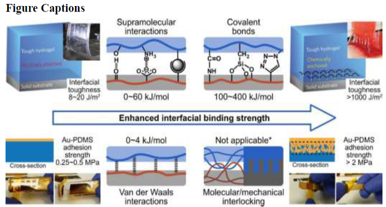
Stretchable electronics are emerging for personalized and decentralized clinics, wearable devices, and human-machine interactions. Nowadays, separated stretchable functional parts have been well developed and approaching practical usage. However, the production of whole stretchable devices with full functions still faces a huge challenge: the integration of different components, which was hindered by the mechanical mismatch and stress/strain concentration at the connection interfaces. To avoid connection failure in stretchable devices, a new research focus is to improve the interfacial binding strength between different components. In this review, recent developments to enhance interfacial strength in wearable/implantable electronics were introduced and catalogued into three major strategies: 1) covalent bonding between different device parts, 2) molecular interpenetration or mechanical interlocking at the interfaces, and 3) covalent connection between the human body and devices. Besides reviewing current methods, we also discussed the existing challenges and possible improvements for stretchable devices from the aspect of interfacial connections. Researcher/Author: Shaobo Ji, Xiaodong Chen (NTU, A*STAR IMRE) National Science Review, nwac172

Non-destructive online seal integrity inspection utilizing autoencoder-based electrical capacitance tomography for product packaging assurance

Publication

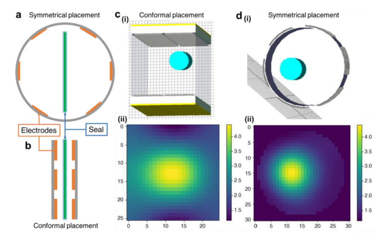
Good quality packaging prevents contamination, secures preservation, and increases the ease of transportation in food and medical industries. One particular weakness of the package lies in the seal region where contents can be unintentionally incorporated, which disrupts the sealing process and compromises the structure and durability of the seal. To validate the seal quality effectively at high speed, a non-destructive high-resolution inspection approach combining enhanced sensors and reconstruction techniques is required. As the seal is flat and defects are minuscule, sensors have to be placed along the contour of the seal to achieve sufficient sensitivity. However, such conformal sensor placement poses new challenges to the ill-posed traditional tomography reconstruction. To overcome the limitation of sensing angle projections, imbalance in pixel representation and physical measurements, and asymmetric geometry of the sensed region, we propose a high-speed supervised autoencoder reconstruction approach. In this paper, our approach achieves high reconstruction image quality of irregular seal regions despite conformal sensor placement. While overcoming the limitations faced in traditional tomography, our model can be seamlessly integrated into the production line for real-time defect detection without affecting production speed and effectively minimizing manufacturing wastage and downtime.

Researcher/Author:Jieming Pan, Zaifeng Yang, Stephanie Hui Kit Yap, Xiangyu Zhang, Zefeng Xu, Yida Li, Yuxuan Luo, Evgeny Zamburg, En-Xiao Liu, Chen-Khong Tham, Aaron Voon-YewThean

Food Packaging and Shelf Life, Volume 33, 2022, 100919

Enabling Active Nanotechnologies by Phase Transition: From Electronics

Publication

Phase transitions can occur in certain materials such as transition metal oxides (TMOs) and chalcogenides when there is a change in external conditions such as temperature and pressure. Along with phase transitions in these phase change materials (PCMs) come dramatic contrasts in various physical properties, which can be engineered to manipulate electrons, photons, polaritons, and phonons at the nanoscale, offering new opportunities for reconfigurable, active nanodevices. In this review, we particularly discuss phase-transition-enabled active nanotechnologies in nonvolatile electrical memory, tunable metamaterials, and metasurfaces for manipulation of both free-space photons and in-plane polaritons, and multifunctional emissivity control in the infrared (IR) spectrum. The fundamentals of PCMs are first introduced to explain the origins and principles of phase transitions. Thereafter, we discuss multiphysical nanodevices for electronic, photonic, and thermal management, attesting to the broad applications and exciting promises of PCMs. Emerging trends and valuable applications in all-optical neuromorphic devices, thermal data storage, and encryption are outlined in the end.

Researcher/Author: Chunqi Zheng (NUS), Robert E. Simpson (SUTD), Kechao Tang (Peking University), Yujie Ke (SUTD), Arash Nemati (ASTAR IMRE), Qing Zhang( University of Electronic Science and Technology of China), Guangwei Hu (NUS), Chengkuo Lee (NUS), Jinghua Teng (ASTAR IMRE), Joel K. W. Yang (SUTD), Junqiao Wu( University of California), Cheng-Wei Qiu (NUS)

Chem. Rev. 2022, 122, 19, 15450–15500

Sub-10nm Ultra-thin ZnO Channel FET with Record-High 561 µA/µm ION at VDS 1V, High µ-84 cm2/V-s and1T-1RRAM Memory Cell Demonstration Memory Implications for Energy-Efficient Deep-Learning Computing

Publication

sub10

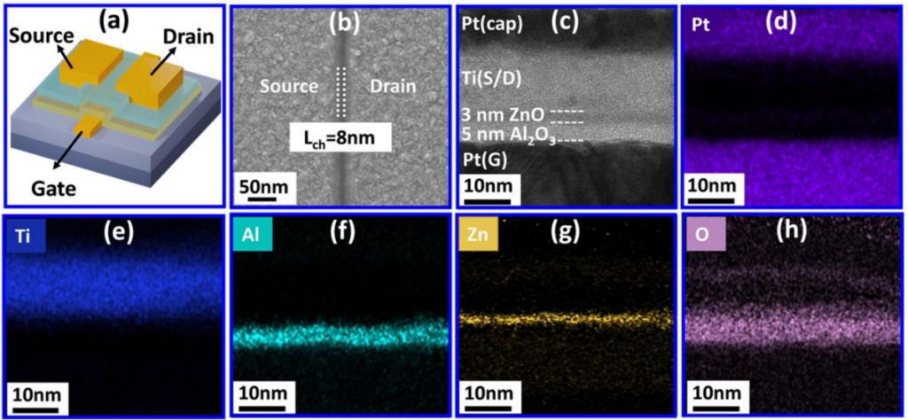
For the first time, we investigated ultra-short-channel ZnO thin-film FETs with L ch = 8 nm with extremely scaled channel thickness t ZnO of 3nm, the device exhibits ultra-low sub-pA/µm off leakage (1.2 pA/µm), high electron mobility (µ eff = 84 cm2/V•s) with record peak transconductance (Gm,) of 254 μS/μm at V DS = 1 V wrt. reported oxide-based transistors, to date, leading to high on-state current (I ON ) of 561 μA/μm. We demonstrated the integration of a ZnO access transistor with Al 2 O 3 RRAM to enable a 1T-1R memory cell, suitable for BEOL-embedded memory. We evaluate the system-level benefits of a hardware accelerator for deep learning to employ FET-RRAM as working memory—up to 10X energy-efficiency benefits can be achieved over current baseline configurations.

Researcher/Author: Umesh Chand, Mohamed M. Sabry Aly+, Manohar Lal, Chen Chun-Kuei, Sonu Hooda, Shih-Hao Tsai, Zihang Fang, Hasita Veluri, Aaron Voon-Yew Thean

2022 IEEE Symposium on VLSI Technology and Circuits (VLSI Technology and Circuits), 2022, pp. 326-327

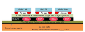
Thermal Challenges and Design Considerations in Heterogeneous Integrated Through-Silicon-interposer Platform for III-V HEMT Flip Chip

Publication

Good quality packaging prevents contamination, secures preservation, and increases the ease of transportation in food and medical industries. One particular weakness of the package lies in the seal region where contents can be unintentionally incorporated, which disrupts the sealing process and compromises the structure and durability of the seal. To validate the seal quality effectively at high speed, a non-destructive high-resolution inspection approach combining enhanced sensors and reconstruction techniques is required. As the seal is flat and defects are minuscule, sensors have to be placed along the contour of the seal to achieve sufficient sensitivity. However, such conformal sensor placement poses new challenges to the ill-posed traditional tomography reconstruction. To overcome the limitation of sensing angle projections, imbalance in pixel representation and physical measurements, and asymmetric geometry of the sensed region, we propose a high-speed supervised autoencoder reconstruction approach. In this paper, our approach achieves high reconstruction image quality of irregular seal regions despite conformal sensor placement. While overcoming the limitations faced in traditional tomography, our model can be seamlessly integrated into the production line for real-time defect detection without affecting production speed and effectively minimizing manufacturing wastage and downtime.

Researcher/Author: Jieming Pan, Zaifeng Yang, Stephanie Hui Kit Yap, Xiangyu Zhang, Zefeng Xu, Yida Li, Yuxuan Luo, Evgeny Zamburg, En-Xiao Liu, Chen-Khong Tham, Aaron Voon-Yew Thean

Food Packaging and Shelf Life, Volume 33, 2022, 100919,

Extremely- Scaled Channel Thickness ZnO FET with High Mobility 86 cm2/V-s, Low SS of 83mV/dec and Low Thermal Budget Process (<300°C)

Publication

In this work, we report a facile approach to significantly improve the electrical performances of a bottom-gated zinc oxide (ZnO) FET through In-situ annealing treatment of ZnO channel layer. We demonstrated ZnO FETs with extremely scaled channel thickness t ZnO of 3 nm, achieving low SS of 83 mV/decade and the highest µeff of 86 cm2/V•s. We offered insights into the sensitive role of interlayer dielectric passivation on oxide device stability, often neglected by prior work.

Researcher/Author: Umesh Chand, Chen Chun-Kuei, Manohar Lal,
Sonu Hooda, Hasita Veluri, Zihang Fang, ShihHao Tsai, Aaron Voon-Yew Thean

2022 6th IEEE Electron Devices Technology & Manufacturing Conference (EDTM), 2022, pp. 256-258

Wafer-scale solution-processed 2D material analog resistive memory array for memory-based computing

Publication

102 photo captured

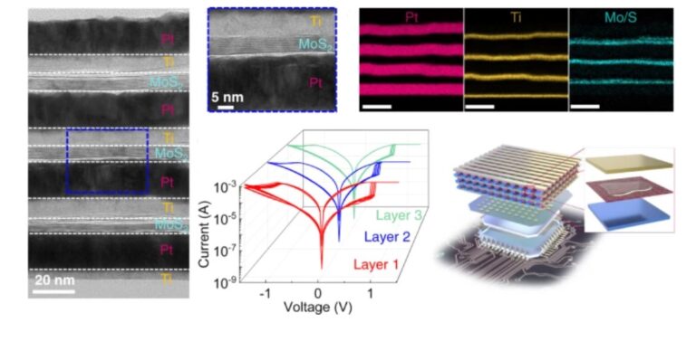
Realization of high-density and reliable resistive random access memories based on two-dimensional semiconductors is crucial toward their development in next-generation information storage and neuromorphic computing. Here, wafer-scale integration of solution-processed two-dimensional MoS2 memristor arrays are reported.

The MoS2 memristors achieve excellent endurance, long memory retention, low device variations, and high analog on/off ratio with linear conductance update characteristics.

The two-dimensional nanosheets appear to enable a unique way to modulate switching characteristics through the inter-flake sulfur vacancies diffusion, which can be controlled by the flake size distribution. Furthermore, the MNIST handwritten digits recognition shows that the MoS2 memristors can operate with a high accuracy of >98.02%, which demonstrates its feasibility for future analog memory applications.

Finally, a monolithic three-dimensional memory cube has been demonstrated by stacking the two-dimensional MoS2 layers, paving the way for the implementation of two memristor into high-density neuromorphic computing system.

Researcher/Author: 

Baoshan Tang,Hasita Veluri, Yida Li, Zhi Gen Yu, Moaz Waqar, Jin Feng Leong, Maheswari Sivan, Evgeny Zamburg, Yong-Wei Zhang, John Wang & Prof Aaron Thean

Published in : Nature Communications on 1 Jun 2022

2.5D-MoS₂-Based Non-Volatile Optical Memory for Integrated Photonics

Publication

Integrated photonics is playing increasingly a key enabling role within optical computing, optical communication, and optical sensing domains. Despite its tremendous versatility, it has some significant limitations for further development and the lack of suitable integrated optical memory is one of them. Over the decade, extensive works have been demonstrated with different optical memory, including Vertical-Cavity Surface-Emitting-Laser (VCSEL) -based optical memory, Phase-Change-Material (PCM)-based optical memory and 2D-material-based Carrier Trapped Optical Memory (CTOM). However, these memory candidates have some shortcomings, in terms of scalability, thermal stability, integration simplicity and so on. In this work, for the first time, we demonstrate an integrated 2.5D-MoS2-based metal-semiconductor-metal (MSM) device to function as a non-volatile optical memory at wavelength of 520nm. 2.5D material is an intermediate state of matter between normal 2D material and bulk crystal. 2.5D MoS2 active material leads to an abrupt resistance switching in optical memory and its switching voltage (VSET) has a high linear correlation to the input light power, which corresponds to “write” operation. To read out the memory, the difference in memory resistance is monitored.

Researcher/Author: Xu Zefeng, Tang Baoshan, Leong Jin Feng, Evgeny Zamburg, Aaron Voon-Yew Thean

2022 Conference on Lasers and Electro-Optics (CLEO)

Artificial Neural Pathway Based on a Memristor Synapse for Optically Mediated Motion Learning

Publication

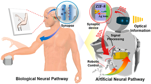
Animals execute intelligent and efficient interactions with their surroundings through neural pathways, exhibiting learning, memory, and cognition. Artificial autonomous devices that generate self-optimizing feedback mimicking biological systems are essential in pursuing future intelligent robots. Here, we report an artificial neural pathway (ANP) based on a memristor synapse to emulate neuromorphic learning behaviors. In our ANP, optical stimulations are detected and converted into electrical signals through a flexible perovskite photoreceptor. The acquired electrical signals are further processed in a zeolitic imidazolate frameworks-8 (ZIF-8)-based memristor device. By controlling the growth of the ZIF-8 nanoparticles, the conductance of the memristor can be finely modulated with electrical stimulations to mimic the modulation of synaptic plasticity. The device is employed in the ANP to implement synaptic functions of learning and memory. Subsequently, the synaptic feedbacks are used to direct a robotic arm to perform responding motions. Upon repeatedly “reviewing” the optical stimulation, the ANP is able to learn, memorize, and complete the specific motions. This work provides a promising strategy toward the design of intelligent autonomous devices and bioinspired robots through memristor-based systems.

Researcher/Author: He Ke, Liu Yaqing, Yu Jiancan, Guo Xintong, Wang Ming, Zhang Liandong, Wan Changjin, Wang Ting, Zhou Changjiu, Chen Xiaodong

ACS Nano 2022, 16, 6, 9691–9700.

  • Home
  • Publications – 2022 – SHINE