Sidebar


Publications – 2025 – SHINE


Bioinspired Heat-Induced Viscoelasticity-Switchable Electrodes for Conformal Brain-Computer Interfaces

Publication

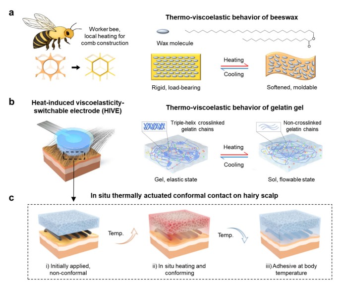
Electroencephalography is a promising noninvasive modality for brain-computer interfaces (BCIs), yet its widespread adoption is constrained by electrode limitations: dry electrodes yield unstable signals, whereas wet electrodes require laborious setup and are ill-suited to wearable devices. Inspired by honeybees that locally heat beeswax to reversibly switch it between rigid and moldable states for comb construction, this work introduces a heat-induced viscoelasticity-switchable electrode (HIVE) that enables conformal contact on hairy scalps and user-friendly operation in wearable systems. HIVE integrates a thermoresponsive gelatin gel confined in a sponge matrix with an on-electrode microheater. Its temperature is actively modulated on demand, enabling autonomous switching between the gel and sol states. As a flowable sol, it permeates hair, conforms to the skin. At body temperature, it remains in a viscoelastic state, providing strong adhesion. Moreover, heating duration is closed-loop controlled using real-time electrode-skin impedance. In steady-state visual evoked potential paradigm, HIVE delivers high classification accuracy comparable to gold-standard wet electrodes while supporting wearable BCI devices for vision-based wheelchair navigation and high-speed text entry. By translating honeybee viscoelasticity-modulation strategy into bioelectronic interfaces, this work provides a practical solution for wearable BCI devices and a new design paradigm for conformal biointerfaces on hairy or piliferous surfaces.

Researcher/Author:  

Zheren Cai, Shangen Zhang, Jianwu Wang, Yifei Luo, Ming Zhu, Zhisheng Lv, Xiaoyang Li, Yuzhen Chen, Yonghao Song, Xiaorong Gao, Cuntai Guan, Xiaodong Chen

Published in: 

Advanced Materials 

Date Added:

28 December 2025

To download the paper, please proceed to:  

DOI: https://doi.org/10.1002/adma.202517936

3D Printable Flexible Composite for Thermal Management of Antennas in Wireless Communication Devices

Publication

 The development of wireless communication technology has resulted in fast and massive data transport. An increase in data traffic entails significant power consumption, which results in problematic heat generation. Thus, the thermal management of wireless communication is crucial. Besides, emerging wearable and soft electronics demand thermally manageable materials with various requirements, such as flexibility, heat dissipation, good dielectric properties, and customized manufacturing. Herein, we introduce a strategy for 3D printable thermal management composite for antennas in wireless communication devices. By employing methacrylate functionalized polydimethylsiloxane (PDMS), we obtained photo-curable PDMS as a 3D printable composite matrix. Paraffin wax-SiO2 (core–shell) particles and 2D Ti3C2Tx MXene are used as fillers, which are excellent heat conductors. Notably, the binary fillers in the composite provided effective thermal transport, resulting in low thermal resistance (0.56 Kcm2/W). Additionally, the composite achieved desirable dielectric properties (dielectric constant: 3.45, loss tangent: 0.0014). With the benefits in 3D printability, heat dissipation performance, and attractive dielectric properties, we fabricated a 3D printed antenna with heat dissipation performance and demonstrated its wireless communication performance.

Researcher/Author: 

Hyunwoo Bark, Chen Gong, Mohammad Ameen, Jae Uk Choi, Adit Gupta, Koen Mouthaan, Pooi See Lee

Published in: Advanced Functional Materials, 2025

Date Added : 24 December 2025

To download the paper, please proceed to:  

DOI: https://doi.org/10.1002/adfm.202525431

Electrically Tunable Edge Defects for Electro-Optic Modulation in WSe2

Publication

Optical modulation is essential for data conversion in optical communication systems, particularly in light of the rapidly increasing data volume and transmission rates, which demand highly energy-efficient modulation technologies. Two-dimensional (2D) material–based optical modulators have emerged as promising candidates; however, their performance is often limited by a trade-off between insertion loss and photon–matter interaction volume. Defect engineering provides a viable strategy to overcome this constraint, as in-gap defect states can prolong carrier recombination lifetimes and thereby enhance modulation efficiency.

In this work, we demonstrate effective modulation of photoluminescence (PL) emission in WSe₂ through electrical carrier injection, which passivates in-gap trap states. This approach establishes a practical pathway for improving the electro-optic performance of 2D material–based modulators.

Researcher/Author: 

Li Jianan

Conference Name : IEEE Semiconductor Interface Specialists Conference (SISC)

Location : San Diego,  USA

Date : 10-13 December 2025

Multiaxis Bendable and Dual-Polarized Antenna Using Closely-Spaced Dual-Corrugated Patches

Publication

A dual-linear polarized quad-element multi-axis conformal antenna for L-band applications is presented. The lightweight and highly conformal antenna is designed by combining flexible copper-cladded polyimide (CCPM) film and PF-4 foam materials. The antenna comprises four dual-corrugated conformal antennas (DCCA), which offer better profile reduction and higher flexibility compared to the single-corrugated conformal antenna (SCCA). Exciting the four ports with different phases generates horizontal polarization (HP) or vertical polarization (VP). The single antenna and quad-element antennas are fabricated and measured for the flat case as well as conformed to a cylinder with radius of 200 mm,160 mm, and 100 mm. For the flat case, the quad-element antenna has a bandwidth of 8.0% (1.281.38GHz) and a boresight gain of 9.4 dBi and 9.2 dBi for VP and HP at 1.32 GHz, respectively.

Researcher/Author: 

Dr Mohammad Ameen and Prof Koen Mouthaan

Published in:  2025 IEEE International Symposium on Antennas and Propagation and North American Radio Science Meeting (AP-S/CNC-USNC-URSI)

Date Added to IEEE Xplore: 08 December 2025

To download the paper, please proceed to:  

DOI: 10.1109/AP-S/CNC-USNC-URSI55537.2025.11266198

Heterogeneous Integration of Performant Lithium Niobate-On-Si Micro-Ring Modulator by High-Precision Micro-Transfer Printing

Publication

We report the first heterogeneous integration of a lithium niobate (LN) micro-ring modulator (MRM) on a silicon photonics platform using a high-precision, back-end-of-line (BEOL)-compatible micro-transfer printing (MTP) technique. Fully fabricated, low-loss LN devices are deterministically aligned and transfer-printed onto CMOS-compatible silicon photonic chips with sub-150 nm placement accuracy and high yield. The resulting hybrid MRM demonstrates an ultra-low insertion loss (<0.6 dB) and a low half-wave voltage–length product (VπL = 1.5 V·cm), achieved through optimized optical waveguide and electrode engineering. The integration scheme supports both lateral (in-plane) and vertical stacking configurations on silicon waveguides, providing versatile integration architectures. Array-level transfer onto foundry-fabricated silicon chips with completed redistribution layer (RDL) interconnects validates the scalability and BEOL compatibility of the process. This non-invasive integration approach addresses critical limitations of conventional LN-on-Si techniques and establishes a viable pathway toward monolithic integration of high-speed photonic I/Os for next-generation optical interconnect systems.

Researcher/Author: 

Yang Jie, Yan Ao

Conference Name : IEEE International Electron Devices Meeting 2025

Location : San Francisco, USA

Date : 6-10 December 2025

Opportunities for 2D-Material-Based Multifunctional Devices and Systems in Bioinspired Neural Networks

Publication

The increasing demand for intelligent, real-time processing is driving artificial intelligence beyond centralized data centers toward distributed, edge-based applications, including autonomous robotics, mobile platforms, and Internet-of-Things (IoT) sensors. However, the energy consumption and form-factor constraints of conventional AI hardware—such as graphics processing units (GPUs) and AI-specific application-specific integrated circuits (ASICs)—pose significant challenges for deployment in resource-limited edge environments. Bioinspired computing paradigms offer a compelling alternative by emulating the efficiency, adaptability, and parallelism of biological neural systems to enable low-power, real-time intelligence. Among these approaches, spiking neural networks (SNNs) are particularly attractive due to their sparse, event-driven operation and have demonstrated orders-of-magnitude improvements in energy efficiency on neuromorphic platforms such as SpiNNaker and Intel’s Loihi. Nevertheless, fully realizing the potential of bioinspired intelligence at the edge necessitates a new class of specialized hardware. Recent advances in materials science, especially the integration of two-dimensional (2D) materials, provide opportunities to develop compact, reconfigurable neuromorphic devices capable of emulating complex neuronal dynamics at ultra-low power. Together, these innovations pave the way for scalable, multifunctional edge AI systems with enhanced capabilities for perception, adaptation, and autonomous decision-making, representing a transformative step toward energy-efficient computing for pervasive intelligent technologies.

Researcher/Author:  

Jin Feng Leong, Maheswari Sivan, Jieming Pan, Zihang Fang, Jianan Li, Zefeng Xu, Shi Zhao, Quanzhen Wan, Evgeny Zamburg, Aaron Voon-Yew Thean

Published in: : Small (2025): e06638 (30 October 2025)

To download the paper, please proceed to:  

DOI:  https://doi-org/10.1002/smll.202506638


Printable Boron Nitride–Liquid Metal Hybrid Thermal Interface Materials for Advanced Electronics

Publication

Efficient thermal management and mechanical flexibility are crucial for modern electronic devices, where compact designs and high power densities generate substantial heat, demanding materials with both high efficiency and excellent conformability. Herein, a hybrid thermal interface material (TIM) exhibiting high thermal conductivity is developed by integrating two-dimensional boron nitride nanosheets (BNNS) and liquid metal (LM) nanoparticles as thermally conductive fillers into a photocurable polydimethylsiloxane (PDMS) matrix. Interfacial engineering of the fillers promotes uniform dispersion and forms a continuous thermal network, enhancing heat transfer while preserving softness. Compared to conventional BN-based 3D-printable TIMs, this hybrid system offers high thermal conductivity and an ultralow Young’s modulus (0.07 MPa), enabling superior conformability on complex surfaces and minimizing thermal contact resistance. The composite also maintains excellent electrical insulation and mechanical stability under repeated deformation, ensuring long-term reliability. Demonstrated in LEDs, batteries, and flexible thermoelectric devices, the BN-LM TIM significantly improves heat dissipation and device performance. This work offers a new strategy that combines optimized filler interactions with DLP 3D printing, bridging efficient heat transport with structural adaptability to advance thermal management in next-generation flexible electronics.

Researcher/Author:

Yixuan Jiang, Hyunwoo Bark, Peiwen Huang, Tan Hu, Yun Li, Pooi See Lee

Published in:   

ACS Publications

Date Added : 18 October 2025

To download the paper, please proceed to:  

DOI:  

https://pubs.acs.org/doi/10.1021/acsami.5c15539?fig=tgr1&ref=pdf

Ferroelectric-Based Pockels Photonic Memory

Publication

Efficient data transfer between memory and photonic components is critical for a broad spectrum of applications. However, conventional architectures face significant challenges related to the memory wall, emphasizing the need for fast, low-energy electro-optic photonic memory solutions. In this work, we present a class of energy-efficient electro-optic devices, termed Pockels photonic memory, which leverage low-field-switchable ferroelectrics in combination with the Pockels effect in lithium niobate.

We detail an integrated implementation consisting of a ferroelectric field-effect transistor (FeFET) coupled with a lithium-niobate-on-insulator (LNOI) microring resonator. The device exhibits switchable, nonvolatile multi-level optical memory operation, supporting six distinct states per transistor with ultra-low energy consumption on the order of femtojoules per state. It also demonstrates robust data retention projected up to 10 years and read–write endurance exceeding 10⁷ cycles. Furthermore, we demonstrate linear stacking of memory states, highlighting the potential for fine-grained optical state control.

The proposed Pockels photonic memory provides a scalable approach to implementing reconfigurable photonic systems with femtojoule-per-state energy efficiency, addressing key bottlenecks in energy- and speed-limited photonic computation.

Researcher/Author: 

Xu Zefeng

Publication  :  Nat Commun 16, 8329 (2025)   

Date : 19 September 2025

Tunable Volatile and Nonvolatile Switching in Silicon Nanosheets Memristor Array for Reservoir Computing

Publication

Reservoir computing (RC) represents a powerful neuromorphic framework for spatiotemporal signal processing. Owing to their intrinsic nonlinear dynamics, memristors are well-suited for RC systems, where volatile devices typically function as the reservoir and nonvolatile devices serve as the readout layer. However, prior implementations have relied on dissimilar, non-silicon materials to realize these two functionalities, leading to significant integration challenges.

Here, we report memristor arrays based on few-layer silicon nanosheets (Si NSs) that enable both volatile and nonvolatile switching within a single material platform, governed by the lateral dimensions of the Si NSs. Devices incorporating small-sized Si NSs exhibit volatile switching with a low set voltage of 0.23 V and stable reservoir dynamics, whereas those based on large-sized Si NSs demonstrate nonvolatile switching with low switching voltages (0.24/–0.18 V) and near-linear conductance modulation. Mechanistic investigations indicate that oxygen vacancies located at nanosheet edges regulate conductive filament dynamics associated with silver ion diffusion, thereby enabling controllable switching volatility. An Si NS-based RC processor is further demonstrated, achieving high accuracy in temporal information processing.

Researcher/Author: 

Xing Chuanwang

Published in: Device, Volume 3, Issue 9, 2025

Date Added : 19 September 2025

3D Printable Flexible Composite for Thermal Management of Antennas in Wireless Communication Devices

Publication

 The development of wireless communication technology has resulted in fast and massive data transport. An increase in data traffic entails significant power consumption, which results in problematic heat generation. Thus, the thermal management of wireless communication is crucial. Besides, emerging wearable and soft electronics demand thermally manageable materials with various requirements, such as flexibility, heat dissipation, good dielectric properties, and customized manufacturing. Herein, we introduce a strategy for 3D printable thermal management composite for antennas in wireless communication devices. By employing methacrylate functionalized polydimethylsiloxane (PDMS), we obtained photo-curable PDMS as a 3D printable composite matrix. Paraffin wax-SiO2 (core–shell) particles and 2D Ti3C2Tx MXene are used as fillers, which are excellent heat conductors. Notably, the binary fillers in the composite provided effective thermal transport, resulting in low thermal resistance (0.56 Kcm2/W). Additionally, the composite achieved desirable dielectric properties (dielectric constant: 3.45, loss tangent: 0.0014). With the benefits in 3D printability, heat dissipation performance, and attractive dielectric properties, we fabricated a 3D printed antenna with heat dissipation performance and demonstrated its wireless communication performance.

Researcher/Author: 

Hyunwoo Bark, Chen Gong, Mohammad Ameen, Jae Uk Choi, Adit Gupta, Koen Mouthaan, Pooi See Lee

Published in: Advanced Functional Materials, 2025

Date Added : 24 December 2025

To download the paper, please proceed to:  

DOI: https://doi.org/10.1002/adfm.202525431

Quantitative Tactile Sensing of Surface Microstructures Through Time-Domain Analysis of Piezoelectric Twin Signals

Publication

Tactile sensors enabling human-like behavior to identify surface microstructures are essential for humanoid robots to interact precisely with complex environments. Most existing approaches use materials responding to dynamic forces and rely on machine learning methods to distinguish various types of surface microstructures. Quantitatively profiling the surface microstructures is significant but challenging, especially under the requirement of eliminating external bulky motion-control systems. Here, a quantitative tactile surface profiling strategy is presented through time-domain analysis of the signal of a piezoelectric twin-film architecture. The architecture uses two parallel piezoelectric films with a fixed interlayer distance, generating twin voltage signals with a time delay, which is inversely proportional to the scanning speed, and consequently removes the need for motion control. The microstructure heights correlate with the peak voltages, whereas widths and edge profiles are derived from the temporal analysis of distinct signal features. Tactile and in situ measurement of surface microstructures is demonstrated with high accuracy (>99.2%) over a broad height range of 1–1000 µm. Furthermore, in-line quality inspection during additive manufacturing is realized by quantitatively profiling the surface microstructures. This work will drive innovations in tactile technologies that emulate and potentially surpass human capabilities and advance in situ surface characterization methods.

Researcher/Author:

Jiaqi Tu, Zheren Cai, Zhihua Liu, Jiangtao Su, Yanzhen Li, Xue Feng, Zequn Cui, Xiaodong Chen

Published in: Advanced Materials

Date Added: 

18 September 2025

To download the paper, please proceed to:  

DOI:

https://doi.org/10.1002/adma.202510393


Engineering Silkworm Silk for Mechanically and Biologically Compliant Skin Electronics

Publication

kin electronics integrated with the human body have attracted significant global interest due to their potential applications in healthcare monitoring and motion sensing. Over the past few decades, electronic devices have become increasingly soft and stretchable with the progress of engineering and materials science, aiming to achieve enhanced integration with the skin and improved acquisition of physiological signals. However, owing to the delicate nature of human skin and its intricate role in regulating body temperature and fluid balance, electronic devices at the skin interface must not only exhibit mechanical compliance but also ensure physiological comfort. They should not block skin metabolism or cause skin damage during daily or long-term use. As a result, the materials used should be biocompatible with the skin/organs without leading to allergic reactions or inflammatory responses. Additionally, these materials should be readily processed into various formats to accommodate skin deformation and breath. As a natural biomaterial, silk is widely acknowledged as the ideal material for developing skin-friendly electronics due to its multifaceted benefits in comparison with many synthetic polymers, including good biocompatibility, tailorable biodegradability, and versatile processability. These properties, which are linked to the conformation of silk, grant silk materials the capacity to be programmed as soft and stretchable as skin. 

Furthermore, silk can be processed through various manufacturing techniques, resulting in diverse material formats like fibers, mats, thin films, hydrogels, and scaffolds that are readily attainable. These rich silk formats exhibit diverse properties and performance characteristics, making them suitable for meeting various requirements in both in vivo and in vitro applications. Leveraging these attributes, natural and regenerated silk materials have been successfully employed in skin-integrated electronics, including but not limited to textile electronics, transient biosensors, adhesive ionic gels, conformal/breathable/stretchable electrodes, and smart dressings. These electronic devices show a high degree of geometric and mechanical compatibility with the skin, and more importantly, they do not cause physical discomfort or disturb skin functions, providing novel prospects for developing high-performance and biologically compliant skin electronics.


In this Account, we highlight recent progress of silk-based materials for skin electronics that prioritize both mechanical and biological compliance. We begin with a comprehensive exploration of the hierarchical structures and inherent properties of natural silk fibers, showing the biocompatibility and biodegradability of silk adapted for bioelectronics, as well as the solution-processability facilitated for the creation of silk materials with versatile formats and properties. Subsequently, we systematically discuss the design and functionality of silk-based skin electronics through engineering structures and materials to fulfill the requirements of high mechanical and biological compliance with the skin. Finally, we elucidate the limitations of current silk-based skin electronics and briefly envision the future challenges and prospects for developing silk as high-performance electronics for comfortable wearing systems.


Researcher/Author: 

Qingsong Li,  Shaobo Ji, Guanglin Li, Zhiyuan Liu, Xiaodong Chen 


Published in: ACS Publications (20 August 2025)


To download the paper, please proceed to:  

DOI:  https://doi.org/10.1021/accountsmr.5c00114


Lightweight Conformal Filtering Antenna Based on Stacking of Multi-Corrugated Polyimide Films

Publication

A lightweight and stacked conformal filtering antenna is demonstrated using copper-cladded polyimide films (CCPF). The antenna consists of primary, secondary, and parasitic patches as rectangular stubs using multi-corrugated polyimide films to improve bending performance. Good filtering performance is obtained by stub-loading of parasitic elements attached to both ends of the primary radiator. Bandwidth (BW) enhancement is achieved by stacking of corrugated polyimide films combined with nylon spacers, forming a five-layer antenna design. For the flat case, the antenna has a BW ranging from 1.17 GHz to 1.38 GHz (16.5%) and nearly flat gain response with a maximum gain of 8.6 dBi at 1.29 GHz. The antenna is fabricated and measured for the flat case and conformed to cylinders with radii Rc200 mm,160 mm,100 mm,80 mm, and 40 mm.

Researcher/Author: 

Dr Mohammad Ameen and Prof Koen Mouthaan

Published in: 2025 IEEE International Conference on Flexible and Printable Sensors and Systems (FLEPS)

Added to IEEE Xplore, 06 August 2025

To download the paper, please proceed to:  

DOI: 10.1109/FLEPS65444.2025.11105666

In-memory Subnet Computation for Area and Energy Efficient AI

Publication

Continual learning at the edge requires energy-efficient hardware capable of dynamic adaptation from limited (few-shot) data, posing fundamental challenges to conventional von Neumann architectures due to data movement overhead and limited parallelism. In this work, we address these challenges by proposing an in-memory computing architecture based on customized dual-gate, back-end-of-line (BEOL) ferroelectric field-effect transistors (FeFETs). Integrated with state-of-the-art subnet-based learning frameworks, the proposed architecture enables energy-efficient multiply–accumulate (MAC) operations while concurrently performing subnet masking, thereby supporting rapid and resource-efficient continual learning.

A single 400 × 100 FeFET crossbar array simultaneously executes MAC and masking operations, achieving at least a 2.42× improvement in energy efficiency. Using this architecture, we obtain an average accuracy of 90.6% across 10 incremental tasks on the Permuted-MNIST (PMNIST) benchmark, comparable to a GPU-based baseline of 91.9%. With increasing model size, the proposed system consistently demonstrates at least 1.39× higher area efficiency and 2.13× faster computation speed relative to state-of-the-art implementations. These results highlight the potential of unconventional in-memory computing architectures to overcome energy, latency, and scalability limitations, paving the way for hardware-realizable continual learning in edge intelligence applications.

Researcher/Author: 

Zhao Shi

Conference Name :AI4X 2025

Location : Singapore

Date : 8-11 July 2025

Bendable Wideband 4 × 4 Dipole Array at X-Band With Adaptive Beamformer for Wide Angle Wireless Sensing

Publication

A low-cost, modular, bendable dipole antenna array with a wide bandwidth is presented for X-band sensing applications. The antenna elements, realized as printed dipoles on a substrate mounted on a ground plane, use a printed balun to enable broadband, balanced excitation. A parasitic dipole is included to increase the bandwidth of the printed dipole. In total, four arrays of four elements each are printed on Rogers RO4350B-based strips to realize the 4 × 4 array. The ground plane is fabricated using thin flexible copper-clad FR-4 substrate, enabling 1-D flexibility. As an example, the array is conformed to a cylinder with a diameter of 12 cm for beamforming. Minimum variance distortionless response beamforming is used and adapted to the wideband conformal array. Experimental results show that the range of beam steering angles can be significantly extended with the proposed design, while keeping sidelobe levels low.

Researcher/Author: 

Prof Koen Mouthaan, Jiahao Wang, Gong Cheng

Published in: IEEE Sensors Letters ( Volume: 9, Issue: 7 July 2025)

To download the paper, please proceed to:  

DOI: 10.1109/LSENS.2025.3575781

A 2-Transistor-1-Modulator (2T1m) Electronic-Photonic Hybrid Memory Architecture for Deep Neural Network Cim and Very Large-Scale Transformers

Publication

Compute-in-memory (CIM) architectures offer a promising approach to improving data-movement efficiency in data-intensive computing workloads, particularly for deep neural networks. However, the scalability of conventional CIM arrays is fundamentally constrained by bitline (BL) IR losses and the associated error accumulation arising from increased wire resistance as array dimensions scale. In this work, we propose a two-transistor–one-modulator (2T1M) electro-optic memory array featuring an optical BL that effectively eliminates BL IR loss and capacitive loading limitations. In each memory cell, dot-product operations are performed using ferroelectric FET (FeFET) devices operating in the subthreshold regime, with the resulting currents accumulated via phase modulation of an optical carrier. An ultra-low-loss, compact lithium-niobate-on-insulator (LNOI) photonic modulator is employed to enable energy-efficient electro-optic conversion. Photonic waveguide BL readout is implemented using pairs of shared Mach–Zehnder interferometers (MZIs) to maximize column-level layout efficiency. By removing BL IR loss, the proposed architecture enables array sizes of up to 3750 kb and achieves up to a 45% improvement in inference accuracy on a large-scale ALBERT transformer model compared with conventional CIM arrays.

Researcher/Author: 

Zhao Shi, Yang Jie, Xu Zefeng

Conference Name : Symposium on VLSI Technology & Circuits 2025

Location : Kyoto, Japan

Date : 8-12 June 2025  

  • Home
  • Publications – 2025 – SHINE